
A multifaceted application of designed coulomb explosion occurring on oxidized topological crystalline insulator SnTe†
Guofeng
Zhang
 * and
Jianbin
Chen
*
* and
Jianbin
Chen
*
Shandong Provincial Key Laboratory of Molecular Engineering, State Key Laboratory of Biobased Material and Green Papermaking, School of Chemistry and Chemical Engineering, Qilu University of Technology (Shandong Academy of Sciences), China. E-mail: zhangguofeng@qlu.edu.cn; jchen@qlu.edu.cn
First published on 2nd December 2021
Abstract
Coulomb explosion, characterized by Coulomb repulsion between particles with the same charge on the surface of a material, has been used to realize exquisite nano-manipulation, however, researchers usually found only one aspect of the application of Coulomb explosion when they utilized it. Herein, we successfully design a “metal@insulator” based Coulomb explosion process by irradiating oxidized topological crystalline insulator SnTe under an electron beam. The occurrence of Coulomb explosion mainly due to the oxide-encapsulated SnTe retained the metallic surface state, which not only can be positively charged but also can realize charge accumulation through the shielding effect of the insulating oxide layer. By changing experimental conditions and carefully studying various experimental phenomena, we conclude six aspects of the application, namely, speculating the metallic surface state of the oxide-encapsulated SnTe, controllable fabricating nanoplates, observing the PVD (physical vapor deposition) process under low temperature, rapid coating film, unraveling the oriented attachment and self-recrystallization of larger nanocrystals and fabricating hollow structure. Our findings are important for utilizing Coulomb explosion as well as other EBI techniques to conduct nano-manipulation.
Introduction
Electron beam irradiation (EBI) has been widely proven to be a powerful technique to engineer nanostructures and modify their physical properties.1,2 When electron beam irradiates materials, some complex processes occur, such as excitation of one or more photons, excitation of plasma, and ejection of the inner- and outer-shell electrons,3 accordingly inducing the heating, sputtering and amorphization of experimental materials, during which one or more mechanisms (e.g., decomposition, kinetic collision and diffusion, formation and motion of vacancies, Coulomb explosion) are involved.4–6 Among those, the Coulomb explosion is an interesting physical phenomenon usually resulting from positive charging, which has been observed in a variety of materials when they are irradiated by an electron beam.7–11 It has been used to exquisitely manipulate nanostructures of some experimental species. For example, Chen et al. fabricated nanoscale Ga balls through a Coulomb explosion that occurred on insulating silica-covered Ga balls when they were irradiated by electron-beam;12 Wang et al. prepared a single copper atom on amorphous carbon via Coulomb explosion;13 Zhang et al. have used Coulomb explosion strategy to tailor nano-architectures of α-MoO3 nanobelts.14 Although these researchers all made excellent use of the Coulomb explosion and obtained interesting scientific results, they only found one aspect of the application of the Coulomb explosion individually.When the Coulomb explosion was used to manipulate nanostructures, the selected experimental species were usually conventional metals or insulators.10,12–14 Topological crystalline insulators, which were discovered in IV−VI semiconductors, such as thermoelectric materials SnTe, Pb1−xSnxSe, and Pb1−xSnxTe,15–19 and featured by a gapless metallic surface state and insulating bulk gap, have never been selected as experimental species for Coulomb explosion studies. So, it is worth expecting whether some interesting phenomenon will occur when their unique electronic band structure is encountered Coulomb explosion.
Herein, we report six aspects of the application of the designed Coulomb explosion that occurred on the oxidized SnTe topological crystalline insulator. The first aspect was demonstrating the metallic state of the inner SnTe, which can be easily realized merely by the successful occurrence of the Coulomb explosion process. Then, by changing the experimental conditions the other five aspects of the application were realized, namely, controllable fabricating nanoplates, observing the PVD (physical vapor deposition) process under low temperature, rapid coating film, unraveling the oriented attachment and self-recrystallization of larger nanocrystals and fabricating the hollow structure. We believe that our work will not only provide some inspiration to fellow readers for more new findings but also can promote the applications of the Coulomb explosion as well as other phenomena based on the EBI technique.
Experimental
Synthetic procedures
Results and discussion
As shown in the scanning electron microscopy (SEM) image (Fig. S1†), the newly prepared SnTe microcrystals presented polyhedral morphology with an angular and smooth surface. The powder X-ray diffraction (XRD) pattern (Fig. S2†) demonstrates the obtained sample was well crystallized pure cubic SnTe, corresponding to the standard JCPDS card No. 46-1210.In order to realize the Coulomb explosion on SnTe, a “metal@insulator” experimental model was adopted as depicted in ref. 12 on the condition that the metallic state of the overlayed SnTe did not change. Then, we exposed the prepared samples in air for about two weeks and six months, guaranteeing the surface of SnTe was encapsulated by oxidized species. The X-ray photoelectron spectroscopy (XPS) spectrum was employed to characterize the oxidized samples. As we can see (Fig. S3 and S4a†), the peak position of C 1s was nearly unchanged when the sample was exposed to air for two weeks and six months, demonstrating that the element C mainly came from the conducting resin. The O 1s of the two samples showed obvious peaks of TeOx and SnO2. As for the Te 3d fitting peaks, we can see that the oxidation products of Te2− were major TeO2 and Te0 when exposed to air for two weeks.20–24 When the exposure time was prolonged to six months, the oxidation products were mainly TeO2, furthermore, the fitting area ratio of TeO2 increased. The Sn 3d fitting peaks clearly demonstrated the oxidation process of SnTe to SnOx.20–24 These obvious changes indicated further oxidization of the surface of SnTe by prolonging the exposure time. After oxidation, the samples were irradiated by the electron beam from the transmission electron microscope (TEM) used in our research.
The actual irradiating results were recorded using time-dependent TEM images. Fig. 1 was recorded using the carbon-supported membrane as a sample holder, exhibiting the evolution process of a sample exposed to air for about two weeks with a 60 s interval. As we can see, the selected area on the sample was nearly unchanged with increasing exposure time and electron beam density, demonstrating that neither thermal explosion nor Coulomb explosion had occurred.
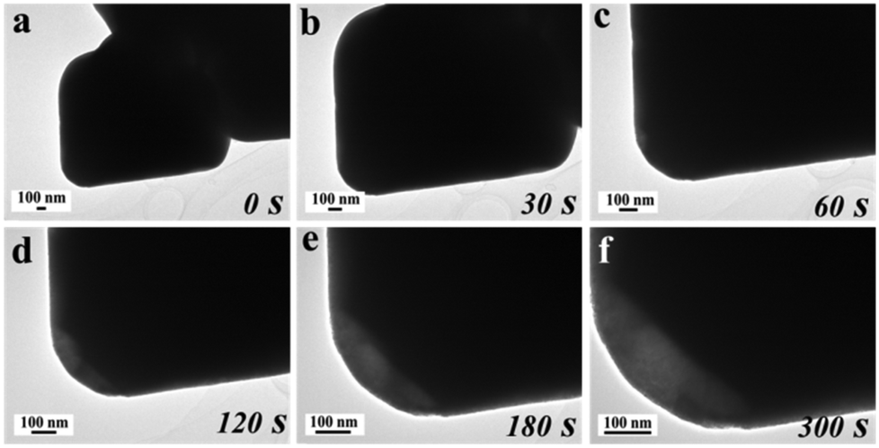 | ||
| Fig. 1 (a–f) Time and beam density-dependent TEM images of irradiating a SnTe sample oxidized in air for two weeks, the corresponding beam densities were 4.5, 6.0, 7.5, 9.0, 10.5 and 12 a cm−2. | ||
When the samples exposed to air for six months were irradiated, the recorded evolution process under an electron beam density of 4.5 A cm−2 (the following experiments also took the value) is as shown in Fig. 2. In the initial period, no obvious change can be observed on the carbon substrate, while, just after 15 s, a noticeable difference from the initial period can be detected and numerous minor nanocrystals or clusters were distributed around the parent body. These nanocrystals grew up to a maximum size of 200 nm rapidly within 180 s, after which they no longer continue to develop with increasing time, leaving a porous thin shell apart, away from the inner solid for about 200 nm. The size of these nanocrystals decreased with increasing distance from the parent body, and the furthest extended distance was about 10 μm (Fig. S5†). The selected area electron diffraction (SAED) shown in Fig. S6† contains only one diffuse set of well-defined concentric rings corresponding to almost all planes of cubic SnTe, indicating that these minor nanocrystals possess phase purity and good crystallinity. The energy-dispersive X-ray spectroscopy (EDS) merely displayed the energy signal of Sn, Te, C and Cu, and no obvious oxygen signals were found (Fig. S7†), further demonstrating SnTe was the only ejected species.25
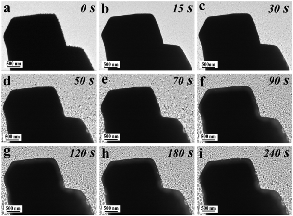 | ||
| Fig. 2 (a–i) Time-dependent TEM images of irradiating a SnTe sample oxidized in air for six months. | ||
Although Te and SnO2 possess excellent conductivity, they still cannot be compared to metal. If the interfacial SnTe retains a metal state, a Coulomb explosion will occur when the electron beam was used to irradiate the model sample, which should be induced by the Coulomb repulsion of accumulated positive charges.7–11 Otherwise, the Coulomb explosion phenomenon cannot be observed, which was due to the nonmetal state SnTe possesses relative to the poor conductivity. Even though the heterostructure may induce electron transfer and rearrangement in the interface, it should not surpass Te and SnO2.
Based on the above experimental results, we can speculate the reason for the occurrence of the Coulomb explosion. When irradiated with the electron beam, SnTe samples were charged followed by charge accumulation. If the accumulated charges cannot be timely transferred away, a Coulomb explosion will occur. In our experiments, we used a carbon-supported membrane as a sample holder, which is a good conductor and can timely transfer away from the generated charge. For the two-week sample, the oxidation layer was thin and not continuous enough (induced by different oxidation rates or ultrasonication for sample customize) to entirely cover the entire sample surface, because the oxidation of SnTe was slow. So, when the two-week sample was irradiated with the electron beam, the generated charge on the oxide surface can be timely transferred away, and the charge generated on the metallic part also can be transferred away through the non-continuous part contact with the carbon-supported membrane. As for the six-month sample, the oxidation layer was thick enough to entirely cover the whole sample surface and not easily shatter by ultrasonication. So, when the six-month sample was irradiated with the electron beam, the generated charge on the oxide surface can be timely transferred away, but the charge generated on the metallic part could not be timely transferred away due to the poor electrical conductivity of the thick oxidation layer (herein we define the phenomenon as shielding effect of the oxide layer). As a result, the charge on the metallic part was continuously accumulated and the repulsion gradually increased. When the repulsion was huge enough to inject SnTe species out of the oxide surface, the Coulomb explosion phenomena occurred.
In brief, we considered that the interior SnTe part experienced a Coulomb explosion process that occurred mainly due to the oxide-encapsulated SnTe retaining the metallic surface state, which not only can be positively charged but also can realize charge accumulation through the shielding effect of the insulating oxide layer in an extremely short irradiating period. In the following, we will present six aspects of the application of the designed Coulomb explosion process.
Speculating on the metallic surface state of the oxide-encapsulated SnTe surface
When it was exposed to air for a long time, the surface of SnTe suffered an oxidation process, and several new species were formed, namely SnO2, TeOx and Te element,21,26 constituting a complicated heterostructure with the inner SnTe part, which may induce the electron transfer and rearrangement in the interface, thereby changing the electronic band structure and influence its topological surface state. Naturally, a problem arose, namely, whether the surface state of the inner part may keep the gapless metallic property or not when the SnTe microcrystals were encapsulated by the oxide layers.As the above experimental results show, the expected Coulomb explosion occurred, so we can consider that the interface should still retain a metallic state and that the interface state has not been influenced by the in situ formed oxide layer. In another case, similar Coulomb explosion processes were observed for various shapes and sizes of nanocrystals (Fig. S8†), indicating the occurrence of the Coulomb explosion process was only dependent on the shielding effect of the oxide layer.
Controllable fabricating nanoplates
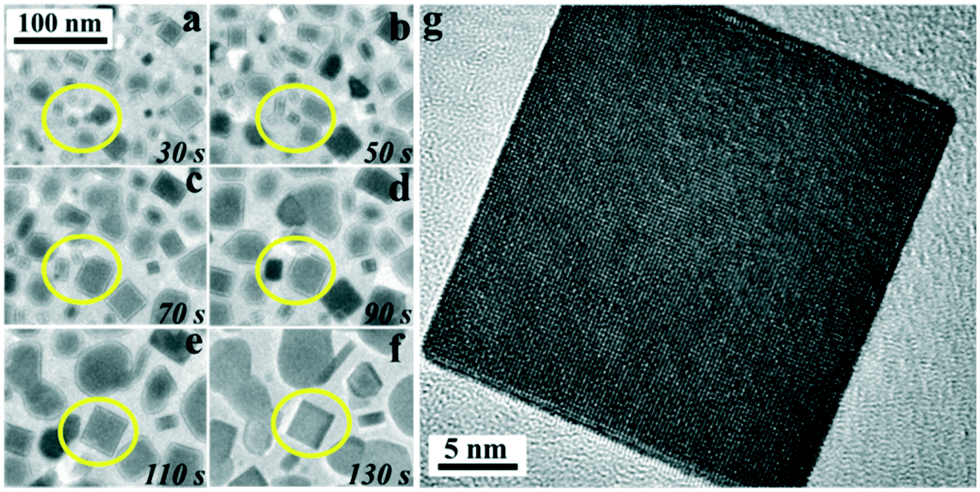
Different crystal surfaces contain their own topological surface states in TCIs, therefore, precisely controlling the morphology of TCIs to obtain particular topological surface states is significant. In various nanostructures, nanoplates show a distinct advantage over others due to the large aspect ratio, which can achieve the selective enhancement of surface states of a particular crystal surface. However, the control fabricating of SnTe nanoplates has rarely been reported, just represented by J. J. Cha's work on the synthesis of SnTe nanoplates with {100} and {111} surfaces through a vapor–liquid–solid growth method using Au as a catalyst.27 The main reason for its difficult to prepare is that SnTe belongs to cubic crystal system, of which the crystal growth orientation determined the preferential extension of a specific crystal plane in two-dimensional direction is hard.Herein, we have used the Coulomb explosion process to synthesize SnTe nanoplates. As demonstrated in the above case at the moment of the 40s, as shown in Fig. 3, we can obtain regular rectangle nanoplates, and that their size distribution characteristic was the same as that at the moment of the 180 s. Although the size of these nanoplates is distributed in a wide range (from several to hundreds of nanometers), it is really a simple and effective method to obtain 2D SnTe nanocrystals, especially the preparation of regular rectangle nanoplates, which differed from usually obtained Coulomb explosion products (balls or irregular particles),12,13 and it should be able to enrich the cognition to the synthesis of 2D materials with a nonlayered crystal structure.
 | ||
| Fig. 3 Representative TEM images of fabricated SnTe nanopaletes as the Coulomb explosion proceeded to 40 s. | ||
Observing the PVD process under low temperature
PVD is a widely used technique to deposit physically vaporized materials to functional film on a targeted substrate in a vacuum, which, usually needs high temperature. The deposition under low temperature has rarely been studied as it usually needs high energy to vaporize common metals, metal alloys, or metal compounds, which was accompanied by generating a huge amount of heat. As we know, a Coulomb explosion usually occurs due to the drastic Coulomb repulsion between the aggregated particles with the same charge, and it can break the bonds that hold solids together. Theoretically, the relatively stationary atoms/molecules on a material surface are emitted as single atoms/molecules under Coulomb repulsion. Unlike thermal ablation, Coulomb explosion is “cold” – it is completed by the time the heat has traveled far enough, moreover, Coulomb explosion usually occurred under a much lower beam density that cannot generate huge heat to vaporize the experimental samples. Therefore, the PVD process under low temperature can be realized through the Coulomb explosion process. Accordingly, the crystallization on the carbon film substrate mentioned above should be a PVD process at low temperatures.In order to study the morphological transformation process during deposition, we have recorded the time-dependent images of the first 40 s in a focused area apart from the parent body for about 1 μm as shown in Fig. 4. Only irradiation initiated for 5 s, the blank carbon film was covered with numerous irregular nanoparticles (Fig. 4a and b), the size of which ranged from less than 1 nm to more than 3 nm. Nearly all of these nanoparticles showed no evidence of crystallization except fewer larger ones (Fig. S9†), among which some smaller cluster-like nanodots were merging into nanoparticles (as shown in the yellow circles), indicating that the initially-ejected SnTe species should be in the shape of single molecules or clusters. After 15 s, SnTe species in the view became denser and larger with some well-configured rectangular nanoplates emerging as shown in Fig. 4e and f, meaning that the nanoparticles should have experienced atomic oriented arrangement and crystallization (Fig. S10†), and we observed that most of the formed nanocrystals showed the same fringe spacing of 0.316 nm, corresponding to the (200) crystal plane of SnTe, which is the lowest energy crystal surface. The transformation seems like the crystallization process in the saturated solution, during which the formation of rectangular morphology of nanocrystals should be resulting from the “NaCl-typed” crystal characteristic of SnTe, but the growth along the z-axis was restrained by the substrate. As marked in the orange circles, some irregular smaller nanoparticles still can be observed in the interstices between the rectangular-shaped nanoplates, indicating the deposition of the ejected single molecules or clusters was a process of “first aggregating, then crystallization”. The next time, with the Coulomb explosion continuously proceeding, the nanoplates rapidly grew up and became thicker with some coalesced, and numerous irregular nanoparticles constantly appeared in the interstices (Fig. 4g and h).
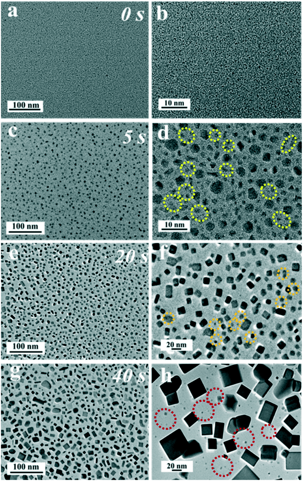 | ||
| Fig. 4 (a–h) Time-dependent TEM images of the deposition process of the ejected SnTe species on the carbon film substrate; right column is the corresponding magnified images of the left. | ||
From the observation results of the deposition process, we can see that the PVD process under low temperature was an analogy to that under high temperature. The difference is that the former is dominated by the kinetic energy transmitting, while the latter is the conduction of heat.
Rapid coating film
Vacuum coating is a mature vacuum application technology, which is based on the techniques operated at high temperatures for the gasification of target materials. It involves vacuum evaporation, vacuum sputtering, vacuum ion plating, vacuum beam deposition and chemical vapor deposition. Using Coulomb explosion to achieve vacuum rapid coating has not been reported, then, herein we will present a case to demonstrate the interesting operation.As described above, we can obtain dispersedly distributed SnTe nanoplates around the parent body along the radial area for several microns. Based on this, if we soak the oxidized parent sample in ethanol for one month, and then properly prolong the ultrasonic treatment time before samples are customized, we can observe a different result as shown in Fig. 5, namely, coating a continuous film. The coating process was motivated just during the process of focusing, and that the parent body was rapidly surrounded by a continuous film just in 10 s. In our opinion, the coating phenomenon was due to the fact that the soaking process and prolonged ultrasonic treatment should have enlarged the porosity (Fig. S12†), which made the eruption of SnTe species much easier and faster. The coating scope can also be extended for more than ten microns apart from the parent body, and the extended distance should rely on the thickness and porosity of the oxidation layer, while it cannot be preciously controlled. Nevertheless, the coating phenomenon can inspire some readers to develop extensive applications using it.
 | ||
| Fig. 5 TEM images of the continuous SnTe film rapidly coated in ∼10 s after focusing the electron beam on the sample: (a) close to the parent body; (b) ∼10 μm away from the parent body. | ||
Unraveling the oriented attachment and self-recrystallization of larger nanocrystals
Oriented attachment is a well-recognized process for crystal growth from primary nanoparticles,28–32 of which the studied sizes were usually small (2–10 nm)33,34 so that they can rotate freely to satisfy the demand for the perfect aligning of their crystallographic orientations parallel to each other for coalescing to a lattice single domain. As for larger nanoparticles, especially for 2D nanoplates, their free rotations were difficult to realize, therefore, the “rotate for parallel aligning” mechanism for coalescing was almost invalid, which should be replaced by the “grain boundary migration” mechanism that generally exists in the sintering process and is controlled by the solute. Therefore, observing the oriented attachment and self-recrystallization of larger nanoparticles using transmission electron microscope was rarely seen in the past research works.Herein, by controlling the Coulomb explosion process, we have realized the in situ observation of the phenomena at low temperatures. Fig. 6 clearly presents the oriented attachment and self-recrystallization of SnTe nanocrystals, whose maximum size approaches 100 nm (circled in orange dotted box). Firstly, we have randomly selected an area (as circled in the yellow box) containing several free-standing minor nanocrystals (in size of 10–20 nm, Fig. 6a) in the initial 30 s of the Coulomb explosion process that occurred on another experiment sample (Fig. S13†). As time goes on, these minor nanocrystals experience growth, oriented attachment, and then self-recrystallizing to a rectangular single crystal domain (Fig. 6b–g). In other selected areas (Fig. S14 and S15†), the oriented attachment and self-recrystallization from more primary nanocrystals can be observed that form larger single crystals.
 | ||
| Fig. 6 (a–f) Time-dependent TEM images of the oriented attachment and self-recrystallization of formed SnTe nanocrystals; yellow circles locked the evolution process of a selected area; (g) HRTEM image of the circled single-crystal SnTe nanoplate in the figure. | ||
In our opinion, after the grain boundary is formed, the ejected SnTe species carry not only energy but also momentum that may reach the surface and grain boundary of the aggregates accompanied by energy transfer. To realize energy minimization, the primary surfaces continuously enlarge by extending the low-energy crystal surfaces dominated by (200). If the aggregates possess minor size as recorded in Fig. 6f, the self-recrystallized single crystals were in the form of a rectangle, otherwise, the morphology is prone to be round-cornered as depicted in Fig. S14f.† As for grain boundaries, their migration and elimination lead to the formation of a single lattice domain, hence after the ejected SnTe species reach the grain boundaries, they carried the energy, and momentum may be transferred to the atoms at grain boundaries, thereby accelerating their migration rate. At last, the atomic arrangements of the high-energy crystal surface were assimilated to that of the contacted low-energy crystal surface, meanwhile, their crystallographic orientations are aligned parallel to each other and then further coalesced. The boundary structure of this case is shown in Fig. 7a, which is in the minority and hard to be founded. If the crystal faces in contact have the same crystallographic orientation but are not perfectly aligned parallel to each other, as shown in Fig. 7b and c, the atoms newly reached to grain boundaries will form an intermediate atomic arrangement state, whose crystallographic orientation is mismatching to a minor extent with the attached two primary crystals (circled in the boxes). Just through the formation of the intermediate state, the grain boundary can continuously migrate and be gradually eliminated, and then the two (or more than two) mismatching primary nanocrystals ultimately coalesced.
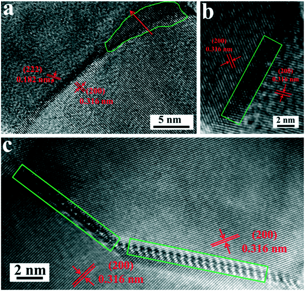 | ||
| Fig. 7 HRTEM images of the grain boundary between two nanocrystals: (a) having different, (b and c) having the same crystallographic orientation; green boxes circled areas present the lattice changing in the grain boundaries. | ||
This section has displayed the oriented attachment and self-recrystallization of larger nanocrystals, which may serve as a supplement for the non-classical theories of crystal growth, meanwhile, it is a reminder for us to pay attention to the influence of energy or momentum of the solute on the growth of crystals in an intermediate or metastable state.
Fabricating hollow structure
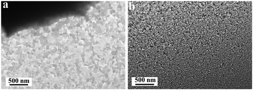
Inorganic micro- and nanosized hollow structures have attracted sustained attention and exhibit potential applications in a number of areas,35–39 due to their well-defined interior voids, low density, large surface area, stability, and surface permeability. Common synthetic strategies for the fabrication of hollow structures include hard templating,40 soft templating,41 selective etching of “soft@hard” particles,42–46 ostwald ripening,47–49 ion exchange50,51 and thermally induced matter relocation methods.52–57 EBI have also been utilized to synthesis hollow structures,58 while using EBI-induced Coulomb explosion to conduct the synthesis of hollow structures have not been reported as far as we know.If we use a micrograte as sample-load support to decrease the conductive efficiency, we can realize the fabrication of the hollow structure. The recorded results under the same electron beam intensity as that of using a carbon-supported membrane as shown in Fig. 8 and S15,† as we can see that the Coulomb explosion process became more violent, which also further demonstrates the metallic state of the interfacial SnTe, meanwhile, we can more intuitively observe the Coulomb explosion process. The whole sample was quickly entirely evacuated and the generated numerous minor nanocrystals coalesced together along the organic films supported on the micrograte, leaving a completely hollow thin conformal shell in about 90 s, which should be the oxide layer. The structural transformation process seems like the transformation of highly crystalline iron–iron oxide core–shell nanoparticles to hollow iron oxide nanostructures in Richard's report,59 in which they attribute the phenomenon to the excess of stabilizing molecules. They thought that these stabilizing molecules created a reasonably thick medium that trapped the incident electrons, leading to a localized, high electron density region that induced a mass transport process within nanomaterials. The difference is that the Coulomb explosion method needs much lower energy. This method may provide new ideas for the nanofabrication of hollow structures using an electron beam or laser technique.
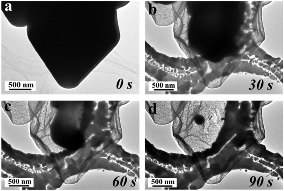 | ||
| Fig. 8 (a–d) Time-dependent TEM images of the forming process of the conformal hollow structure. | ||
Conclusions
In summary, we have realized multifaceted applications of the designed Coulomb explosion model for six aspects, namely, speculating on the metallic surface state of oxide-encapsulated SnTe, controllable fabricating nanoplates, observing the PVD process under low temperature, rapid coating film, unraveling the oriented attachment and self-recrystallization of larger nanocrystals and fabricating hollow structures by changing various experimental conditions. Although we merely, concisely, described the six-aspect application, the perspectives of thinking in our report may inspire some researchers to develop new and interesting utilisations of the Coulomb explosion as well as other EBI techniques.Conflicts of interest
The authors declare no competing financial interest.Acknowledgements
We greatly appreciate the financial support from the National Natural Science Foundation of China (No. 22171154 and 21801144), the Youth Innovative Talents Recruitment and Cultivation Program of Shandong Higher Education, the Natural Science Foundation of Shandong Province (No. ZR2020QB114, ZR2020QB008 and ZR2018BB017), Qilu University of Technology (Shandong Academy of Sciences). The project supported by the Foundation (No. ZZ20190312) of State Key Laboratory of Biobased Material and Green Papermaking, Qilu University of Technology (Shandong Academy of Sciences), and the Program for Scientific Research Innovation Team in Colleges and Universities of Shandong Province.References
- Krasheninnikov and F. Banhart, Nat. Mater., 2007, 6, 723–733 CrossRef CAS PubMed
.
- A. V. Krasheninnikov and K. Nordlund, J. Appl. Phys., 2010, 107, 3–127 CrossRef
- M. Dapor, Springer Tracts Mod. Phys., 2003, 186, 1–4 Search PubMed
- H. Duan, E. Xie, L. Han and Z. Xu, Adv. Mater., 2008, 20, 3284–3288 CrossRef CAS
- I. Last and J. Jortner, J. Chem. Phys., 2004, 121, 8329–8342 CrossRef CAS PubMed
- J. Lin, O. Cretu, W. Zhou, K. Suenaga, D. Prasai, K. I. Bolotin, N. T. Cuong, M. Otani, S. Okada, A. R. Lupini, J. C. Idrobo, D. Caudel, A. Burger, N. J. Ghimire, J. Yan, D. G. Mandrus, S. J. Pennycook and S. T. Pantelides, Nat. Nanotechnol., 2014, 9, 436–442 CrossRef CAS PubMed
- K. Sattler, J. Mühlbach, O. Echt, P. Pfau and E. Recknagel, Phys. Rev. Lett., 1981, 47, 160–163 CrossRef CAS
- Z. Vager, R. Naaman and E. P. Kanter, Science, 1989, 244, 426–431 CrossRef CAS PubMed
- S. Chelkowski, P. B. Corkum and A. D. Bandrauk, Phys. Rev. Lett., 1999, 82, 3416–3419 CrossRef CAS
- X. Wei, D. M. Tang, Q. Chen, Y. Bando and D. Golberg, ACS Nano, 2013, 7, 3491–3497 CrossRef CAS PubMed
- B. Gross, H. von Seggern and J. E. West, J. Appl. Phys., 1984, 56, 2333–2336 CrossRef CAS
- Y. Chen, Y. Huang, N. S. Liu, J. Su, L. Y. Li and Y. H. Gao, Sci. Rep., 2015, 5, 11313 CrossRef CAS PubMed
- K. Wang, H. Wu, W. Yuan, W. Xi and J. Luo, Nanoscale, 2019, 11, 7595–7599 RSC
- J. Zhang, L. Zhu, Y. Yang, H. Yong, J. Zhang, Y. Peng and J. Fu, Nanoscale, 2018, 10, 8285–8291 RSC
- T. H. Hsieh, H. Lin, J. Liu, W. Duan, A. Bansil and L. Fu, Nat. Commun., 2012, 3, 982 CrossRef PubMed
- Y. Tanaka, Z. Ren, T. Sato, K. Nakayama, S. Souma, T. Takahashi, K. Segawa and Y. Ando, Nat. Phys., 2012, 8, 800–803 Search PubMed
- P. Dziawa, B. J. Kowalski, K. Dybko, R. Buczko, A. Szczerbakow, M. Szot, E. Tusakowska, T. Balasubramanian, B. M. Wojek, M. H. Berntsen, O. Tjernberg and T. Story, Nat. Mater., 2012, 11, 1023–1027 CrossRef CAS PubMed
- S. Y. Xu, C. Liu, N. Alidoust, M. Neupane, D. Qian, I. Belopolski, J. D. Denlinger, Y. J. Wang, H. Lin, L. A. Wray, G. Landolt, B. Slomski, J. H. Dil, A. Marcinkova, E. Morosan, Q. Gibson, R. Sankar, F. C. Chou, R. J. Cava, A. Bansil and M. Z. Hasan, Nat. Commun., 2012, 3, 1192 CrossRef PubMed
- Y. Tanaka, T. Shoman, K. Nakayama, S. Souma, T. Sato, T. Takahashi, M. Novak, K. Segawa and Y. Ando, Phys. Rev. B: Condens. Matter Mater. Phys., 2013, 88, 330–339 Search PubMed
- M. Saghir, M. Walker, C. F. McConville and G. Balakrishnan, Appl. Phys. Lett., 2016, 108, 061602 CrossRef
- V. S. Neudachina, T. B. Shatalova, V. I. Shtanov, L. V. Yashina, T. S. Zyubina, M. E. Tamm and S. P. Kobeleva, Surf. Sci., 2005, 584, 77–82 CrossRef CAS
- Y. Y. Wang, K. F. Cai and X. Yao, Appl. Surf. Sci., 2011, 258, 919–922 CrossRef CAS
- C. H. An, K. B. Tang, B. Hai, G. Z. Shen, C. R. Wang and Y. T. Qian, Inorg. Chem. Commun., 2003, 6, 181–184 CrossRef CAS
- S. H. Gu, K. Ding, J. Pan, Z. B. Shao, J. Mao, X. J. Zhang and J. S. Jie, J. Mater. Chem. A, 2017, 5, 11171–11178 RSC
- G. J. Tan, L. D. Zhao, F. Y. Shi, J. W. Doak, S. H. Lo, H. Sun, C. Wolverton, V. P. Dravid, C. Uher and M. G. Kanatzidis, J. Am. Chem. Soc., 2014, 136, 7006–7017 CrossRef CAS PubMed
- N. Berchenko, R. Vitchev, M. Trzyna, R. Wojnarowska-Nowak, A. Szczerbakow, A. Badyla, J. Cebulski and T. Story, Appl. Surf. Sci., 2018, 452, 134–140 CrossRef CAS
- J. Shen, Y. W. Jung, A. S. Disa, F. J. Walker, C. H. Ahn and J. J. Cha, Nano Lett., 2014, 14, 4183–4188 CrossRef CAS PubMed
- J. F. Banfield, S. A. Welch, H. Zhang, T. T. Ebert and R. L. Penn, Science, 2000, 289, 751–754 CrossRef CAS PubMed
- R. L. Penn and J. F. Banfield, Science, 1998, 281, 969–971 CrossRef CAS PubMed
- R. L. Penn and J. F. Banfield, Am. Mineral., 1998, 83, 1077–1082 CrossRef CAS
- R. L. Penn and J. F. Banfield, Geochim. Cosmochim. Acta, 1999, 63, 1549–1557 CrossRef CAS
- D. Li, M. H. Nielsen, J. R. I. Lee, C. Frandsen, J. F. Banfield and J. J. D. Yoreo, Science, 2012, 336, 1014–1018 CrossRef CAS PubMed
- J. Lee, J. W. Yang, S. G. Kwon and T. W. Hyeon, Nat. Rev. Mater., 2016, 1, 16034 CrossRef CAS
- C. Zhu, S. X. Liang, E. H. Song, Y. J. Zhou, W. Wang, F. Shan, Y. T. Shi, C. Hao, K. B. Yin, T. Zhang, J. J. Liu, H. M. Zheng and L. T. Sun, Nat. Commun., 2018, 9, 421 CrossRef PubMed
- F. Caruso, Chem. – Eur. J., 2000, 6, 413–419 CrossRef CAS
- K. Kamata, Y. Lu and Y. N. Xia, J. Am. Chem. Soc., 2003, 125, 2384–2385 CrossRef CAS PubMed
- C. E. Fowler, D. Khushalani and S. Mann, Chem. Commun., 2001, 2028–2029 RSC
- Y. Wan and D. Y. Zhao, Chem. Rev., 2007, 107, 2821–2860 CrossRef CAS PubMed
- H. Cölfen and M. Antonietti, Angew. Chem., Int. Ed., 2005, 44, 5576–5591 CrossRef PubMed
- F. Caruso, R. A. Caruso and H. Mohwald, Science, 1998, 282, 1111–1114 CrossRef CAS PubMed
- X. W. Lou, L. A. Archer and Z. C. Yang, Adv. Mater., 2008, 20, 3987–4019 CrossRef CAS
- Q. Zhang, T. R. Zhang, J. P. Ge and Y. D. Yin, Nano Lett., 2008, 8, 2867–2871 CrossRef CAS PubMed
- D. Chen, L. L. Li, F. Q. Tang and S. O. Qi, Adv. Mater., 2009, 21, 3804–3807 CrossRef CAS
- X. J. Wu and D. S. Xu, Adv. Mater., 2010, 22, 1516–1520 CrossRef CAS PubMed
- Z. G. Teng, X. D. Su, Y. Y. Zheng, J. Sun, G. T. Chen, C. C. Tian, J. D. Wang, H. Li, Y. N. Zhao and G. M. Lu, Chem. Mater., 2013, 25, 98–105 CrossRef CAS
- Z. G. Teng, S. J. Wang, X. D. Su, G. T. Chen, Y. Liu, Z. M. Luo, W. Luo, Y. X. Tang, H. X. Ju, D. Y. Zhao and G. M. Lu, Adv. Mater., 2014, 26, 3741–3747 CrossRef CAS PubMed
- W. Z. Ostwald, Phys. Chem., 1900, 34, 495–503 Search PubMed
- H. G. Yang and H. C. Zeng, J. Phys. Chem. B, 2004, 108, 3492–3495 CrossRef CAS
- L. Zhang and H. Wang, J. Phys. Chem. C, 2011, 115, 18479–18485 CrossRef CAS
- S. L. Xiong and H. C. Zeng, Angew. Chem., Int. Ed., 2012, 124, 973–976 CrossRef
- L. F. Shen, L. Yu, H. B. Wu, X. Y. Yu, X. G. Zhang and X. W. Lou, Nat. Commun., 2015, 6, 6694 CrossRef CAS PubMed
- L. Zhou, D. Zhao and X. W. Lou, Adv. Mater., 2012, 24, 745–748 CrossRef CAS PubMed
- W. Cho, Y. H. Lee, H. J. Lee and M. Oh, Adv. Mater., 2011, 23, 1720–1723 CrossRef CAS PubMed
- G. Q. Zhang, L. Yu, H. B. Wu, H. E. Hostera and X. W. Lou, Adv. Mater., 2012, 24, 4609–4613 CrossRef CAS PubMed
- L. F. Shen, L. Yu, X. Y. Yu, X. G. Zhang and X. W. Lou, Angew. Chem., Int. Ed., 2015, 54, 1868–1872 CrossRef CAS PubMed
- X. Y. Lai, J. Li, B. A. Korgel, Z. H. Dong, Z. M. Li, F. B. Su, J. A. Du and D. Wang, Angew. Chem., Int. Ed., 2011, 50, 2738–2741 CrossRef CAS PubMed
- J. G. Guan, F. Z. Mou, Z. G. Sun and W. D. Shi, Chem. Commun., 2010, 46, 6605–6607 RSC
- L. Y. Lian, F. Cheng, Y. Xia, M. Y. Zheng, J. P. Ke, W. Z. Zhang, J. G. He, H. Liu, D. L. Zhang, J. B. Gao, J. Tang, L. M. Li, M. L. Tan and J. B. Zhang, J. Phys. Chem. C, 2018, 122, 49 Search PubMed
- D. A. J. Herman, S. S. Cheong, M. J. Banholzer and R. D. Tilley, Chem. Commun., 2013, 49, 6203–6205 RSC
Footnote |
| † Electronic supplementary information (ESI) available: XRD, XPS spectra, SEM and TEM images. See DOI: 10.1039/d1ce01343b |
| This journal is © The Royal Society of Chemistry 2022 |