
Phase B vanadium dioxide: characteristics, synthesis and applications
Yujing
Zhang
,
Nan
Chen
,
Yang
Zhou
*,
Haojie
Lai
,
Pengyi
Liu
and
Weiguang
Xie
 *
*
Guangdong Provincial Engineering Technology Research Center of Vacuum Coating Technologies and New Energy Materials, Jinan University, Guangzhou 510632, People's Republic of China. E-mail: yangzhou@email.jnu.edu.cn; wgxie@email.jnu.edu.cn
First published on 29th November 2021
Abstract
VO2(B) is a metastable phase of VO2 composed of both edge and corner sharing irregular VO6 octahedrons. As a metallic phase at room temperature, VO2(B) exhibits large tunnels in the lattices that allow the rapid intercalation and deintercalation of metal ions. It also shows a high temperature coefficient of resistance (TCR) and low 1/f noise with appropriate resistance. These merits attract much attention in the field of metal ion batteries and uncooled infrared detectors. In this passage, advances in the development of the preparation and applications of VO2(B) are systematically reviewed. We focus on the structure and properties of VO2(B) that strongly affect its applications in metal ion batteries, uncooled infrared detectors and gas sensors, together with the way of controlling them in different preparation methods. A new application in gas and humidity sensing is also mentioned. Finally, we briefly discuss the possible directions of VO2(B) materials in future research, hoping that this article can provide a valuable reference for research on VO2(B) in the future.
 Yujing Zhang | Yujing Zhang received his Bachelor's degree from Jinan University in 2019. Currently, he continues to study for a Master's degree at Jinan University under the supervision of Prof. Weiguang Xie. His current research focuses on vanadium dioxide prepared by the hydrothermal method and its applications in uncooled infrared detection and terahertz detection. |
 Nan Chen | Nan Chen is an undergraduate in the Department of Physics, Jinan University, Guangzhou, Guangdong, China. Her current research focuses on the growth mechanism and preparation of controlled vanadium oxide nanomaterials and their applications in optoelectronic properties. |
 Yang Zhou | Dr. Yang Zhou received his BSc degree in materials science from University of Science and Technology of China in 2011 and received his PhD degree from School of Materials Science and Engineering at Nanyang Technological University in 2016. After two-year postdoctoral research at Nanyang Technological University, he is currently working at Jinan University. His research interest is focused on optoelectrical and piezoelectric/ferroelectric materials. |
 Haojie Lai | Haojie Lai received his Master's degree from Jinan University in 2020. Currently, he continues to study for a doctoral degree at Jinan University under the supervision of Prof. Weiguang Xie. His current research focuses on the photoelectric detection of two-dimensional materials. |
 Pengyi Liu | Prof. Pengyi Liu received his PhD from Sun Yat-sen University in 2005. He is a professor of the Department of Physics, and Vice Dean of School of Science and Technology in Jinan University. He mainly engages in vacuum technology and thin film materials research, including functional thin film technology, photoelectric materials and devices, and solar cells. Prof. Liu has published over 50 research papers, and filed 4 patents. He has won the second prize of the Science and Technology Award of the China Association for Instrumental Analysis in 2020. |
 Weiguang Xie | Prof. Weiguang Xie received his PhD from Sun Yat-sen University in 2008. He is now a professor at Jinan University. His main research interests cover the optoelectrical properties and application of van der Waals materials and perovskite materials. Prof. Xie has published over 90 research papers, and filed 8 patents. He has won the first prize of the Science and Technology Award of the Chinese Association for Analysis and Testing in 2016, and the second prize of Science Technology Improvement Award at a higher institution in China in 2014. |
1. Introduction
Vanadium (V), which has the ground state electronic configuration of [Ar]3d34s2, is the fifth most abundant transition metal on Earth. Its content accounts for about 0.02% of the earth's crust. V exists in numerous possible valence states; thus, it has many different oxides.1 Vanadium oxides such as VO, V2O3, VO2 and V2O5 exist in a single oxidation state, whereas many others, for instance, V3O5, V4O7, V6O11, V6O13, V7O13, and V8O15, remain in mixed (two) valence states. Among them, V2O3, VO2 and V2O5 have been widely studied as optical, electrical, electrochemical, thermochromic and thermal-switching materials.2 VO2, in particular, has received great attention due to its multiple structure phases and unique optical and electrical properties.3 So far, several VO2 crystal phases have been reported, including tetragonal VO2(R) (P42/mnm),4 monoclinic VO2(M) (P21/c),5,6 tetragonal VO2(A) (P42/nmc),7 single oblique VO2(B) (C2/m)8 and triclinic VO2(T) (P*(2)).9Among the various phase states of VO2, VO2(M) and VO2(R) have attracted much attention in applications such as smart windows and photoelectric conversion switches due to their reversible metal–insulator transition between the two phases. VO2(A) is an unstable intermediate phase. It usually occurs between the phase transition process from VO2(B) to VO2(R).7,10 VO2(B) is a material with a metastable monoclinic structure. It has been applied in many fields, including energy conversion and storage,11–13 uncooled infrared detectors,14–16 as well as gas and humidity sensors.17–19
In the current study of VO2(B), the most popular and widely reported applications are metal ion batteries and uncooled infrared detectors. At room temperature, VO2(B) is in the metallic phase, which is required for superior electrical transport. The tunnel structure of VO2(B) can be utilized as a large diffusion channel for the rapid intercalation and deintercalation of metal ions,20,21 enabling ions to intercalate and de-intercalate in a reversible metal ion battery.22,23 For uncooled infrared detectors, VO2(B) has no obvious phase change at room temperature, no sudden changes in electrical and optical parameters, and no thermal hysteresis. The 1/f noise is low and its TCR is high. These advantages are beneficial as a thermal sensitive material for uncooled infrared detectors.
In recent years, gratifying progress has been made in the research on VO2(B). Several reviews8,24,25 have mentioned VO2(B) and recognized the achievements of VO2(B) in the corresponding fields. However, these reviews just mentioned part of the features of VO2(B) rather than introducing it systematically or in detail. Therefore, in this review, we aim at making a detailed summary of VO2(B). The first chapter gives an overview on the structural and opto-electrical properties of VO2(B). The second chapter will specifically introduce the major preparation methods of VO2(B), mainly to control the structure and properties. The advantages and disadvantages of different methods will be discussed. The third chapter will outline the popular applications of VO2(B) at present. The fourth chapter will summarize and look forward to the future of VO2(B). We hope that this review can provide a reference for those who are working on the application of VO2(B), and also make a little contribution to the fundamental research on oxide materials.
2. The structure and properties of VO2(B)
VO2(B) is a metastable monoclinic phase of VO2 belonging to the space group C2/m, as shown in Fig. 1a.26–28 In 1975, Théobald et al.26 reported the structure of VO2(B) powder for the first time. At room temperature, the crystallographic parameters of VO2(B) are a = 12.0414 Å, b = 3.6892 Å, c = 6.4299 Å, and β = 106.95°. The specific structural parameters and atomic coordinates are shown in Table 1.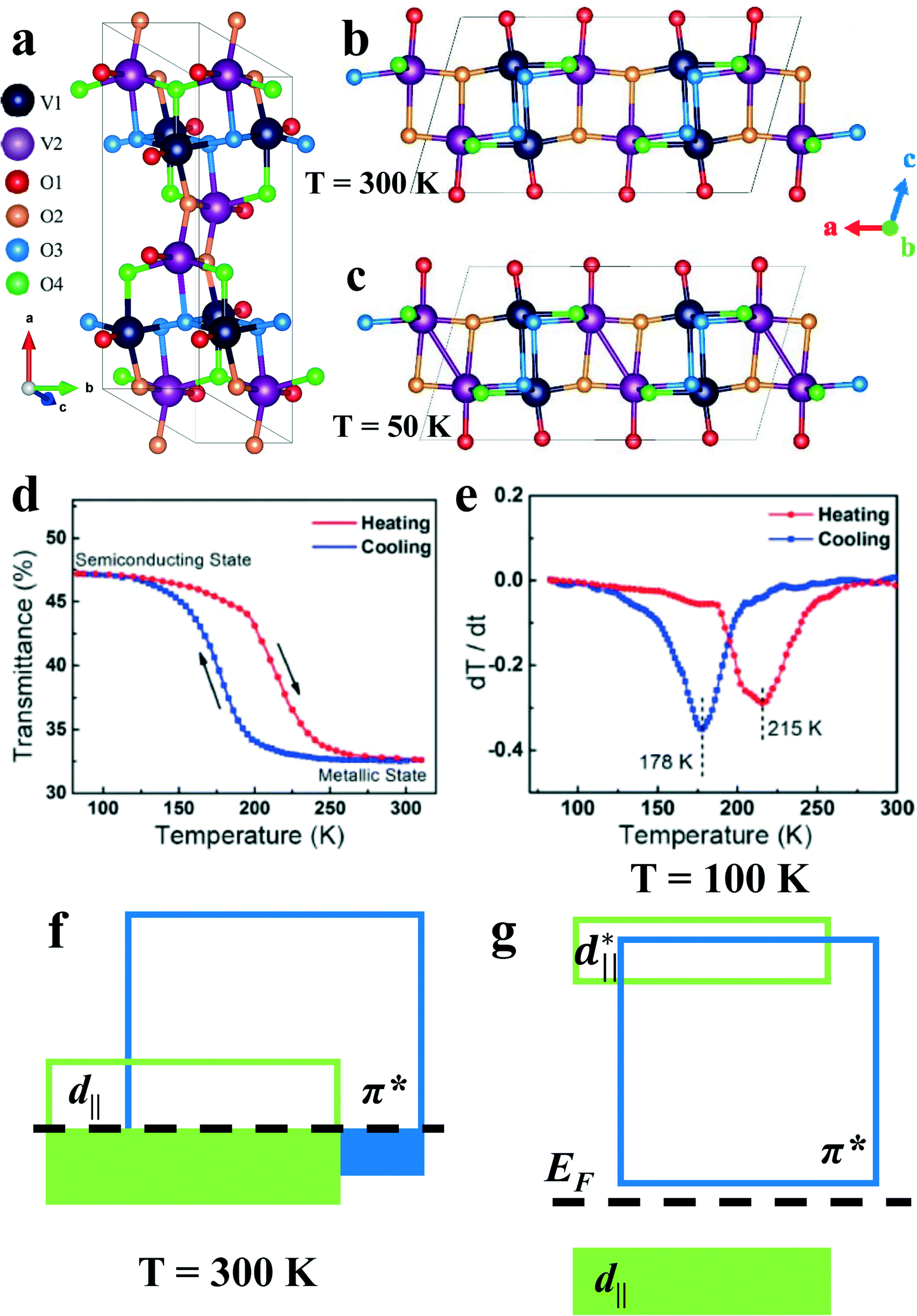 | ||
| Fig. 1 a) Schematic of the crystal structure of VO2(B). The metastable and monoclinic deformation of VO2(B) at b) 300 K and c) 50 K. d) Temperature-dependent transmittance hysteresis at 1600 nm wavelength illumination. e) Differential curves (dT/dt) of the transmittance curve in d). Reproduced with permission.29 Copyright 2018, Japanese Journal of Applied Physics. Schematic diagram of the VO2(B) band structure of f) the metallic phase (300 K) and g) the insulating phase (100 K). Reproduced with permission.30 Copyright 2016, Scientific Reports. | ||
| Atom label | Wyckoff position | Atomic coordinates | Occupancy | |
|---|---|---|---|---|
| x | z | |||
| V1 | 4i | 0.3046(2) | 0.7228(4) | 1 |
| V2 | 4i | 0.4031(2) | 0.3044(4) | 1 |
| O1 | 4i | 0.3692(6) | 0.998(1) | 1 |
| O2 | 4i | 0.2340(7) | 0.330(1) | 1 |
| O3 | 4i | 0.4465(6) | 0.648(1) | 1 |
| O4 | 4i | 0.1313(6) | 0.697(1) | 1 |
Similar to the case of VO2(M) and VO2(R), where there is a metal-insulation transition at 68 °C,31 VO2(B) undergoes a structural transformation below room temperature, which is accompanied by abnormal magnetic susceptibility. Through X-ray powder diffraction studies, Oka et al.32 determined that the structural transformation of the compound was caused by V4+–V4+ dimerization. The structure of VO2(B) at high temperature (300 K) and low temperature (50 K) measured by Oka et al. are shown in Fig. 1b and c, respectively.33 During the high-temperature to low-temperature phase transition, the monoclinic space group does not change, mainly due to the formation of non-magnetic V–V pairs between the V(2) atoms. With the increase in the paramagnetic V atoms in all high temperature phases (HTP) and low temperature phases (LTP), the V(2)–V(2) bond is similar to that in rutile VO2, and the covalent bond formation with the decrease in the temperature leads to V4+–V4+ pairing. Specific examples are shown in Tables 2 and 3. One of the manifestations is the change in the transmittance in this temperature range, as shown in Fig. 1d and e. It can be found that, compared with the HTP, the lattice along the x- and z-axis, which matches a-axis and c-axis, respectively, changes more obviously in the LTP. Analyzing the band structures of HTP and LTP (Fig. 1f and g), it could be found that the LTP of VO2(B) has a larger d∥ band split, and the π* band also moves to a relatively higher energy.30 In the HTP, the energy bands coincide at the Fermi level, which is the reason that VO2(B) exhibits a certain metal-like property at room temperature.
| HTP | LTP | |
|---|---|---|
| T/K | 300 | 50 |
| Space group | C2/m | C2/m |
| a/Å | 12.0414(4) | 12.152(2) |
| b/Å | 3.6892(1) | 3.7199(5) |
| c/Å | 6.4299(2) | 6.347(1) |
| β/° | 106.95 | 107.58(3) |
| V/Å3 | 273.23(2) | 273.5(2) |
| HTP | LTP | |
|---|---|---|
| Symmetry codes: i x, 0, z; ii 1 − x, 0, 1 − z; iii 1/2 + x, 1/2, z; iv 1/2 − x, 1/2, 1 − z. | ||
| V(1)i–V(1)iv | 0.3319(4) | 0.3307(6) |
| V(1)i–V(2)ii | 0.3177(4) | 0.3169(6) |
| V(1)i–V(2)iv | 0.3005(4) | 0.3002(6) |
| V(2)i–V(2)ii | 0.2867(4) | 0.2670(7) |
In addition to the temperature dependence of the phase change of VO2(B)29 (Fig. 1d and e), there is also a phase change controlled by the luminous flux at a certain temperature30 (Fig. 2a and b). Applying a certain amount of light influence to VO2(B) in the LTP until the critical luminous flux threshold (Fth) is exceeded, the insulating state will change to a metallic state. The Fth value, in accordance with the experimental data of luminous flux and temperature, can draw the boundary phase (Fig. 2c).30 The red- and the blue-shaded regions represent the metallic state and the insulating states, respectively. The region (I) of the red and blue streaks represents the insulation-metal transition state with a longer thermal relaxation time. The reason VO2(B) stays in the region (I) is that the pure laser energy or low-temperature heat cannot make the system reach region (II) of metallic state. Thus, when the laser energy and system temperature rise, VO2(B) changes to the metallic state. The width of region (I) decreases with increasing temperature, which is a manifestation of this mechanism.
 | ||
| Fig. 2 Values of a) A and b) tp for the VO2(B) film as a function of fluence. The positive A corresponds to the insulating state of VO2(B), while the negative A corresponds to the metallic state. The tp is defined as the time delay where ΔR/R reaches a maximum immediately following optical excitation. The Fth of 1.5 mJ cm−2 at 150 K is indicated by the black arrow in a). c) Summary of the dynamics study of VO2(B), as represented by the phase diagram. Reproduced with permission.30 Copyright 2016, Scientific Reports. | ||
According to the literature,34–36 the V2p peak splits into V2p1/2 and V2p3/2. The binding energy of the V5+2p3/2 peak is located in the range of 516.9–517.7 eV. The binding energy of the V4+2p3/2 peak is located in the range of 515.7–516.2 eV. The binding energy of the V3+2p1/2 peak is located near 523 eV. Fig. 3a shows the core-level spectra of V2p of the VO2(B) center at 515.56 eV, 517.1 eV and 522.8 eV, showing that all the V atoms are at +4 states. The valence spectrum of VO2(B) is shown in Fig. 3b. There is a large band in the range of 2–10 eV, which is mainly attributed to the O-2p orbital. At 0–2 eV, Choi et al.15 shows the existence of the occupied band for VO2(B) at room temperature, which is primarily dominated by the V-3d orbitals. Compared with V2O5, it is found that the band tail of V-3d of VO2(B) and V6O13 crosses the Fermi level, which is consistent with the metallic properties of VO2(B) at room temperature.37
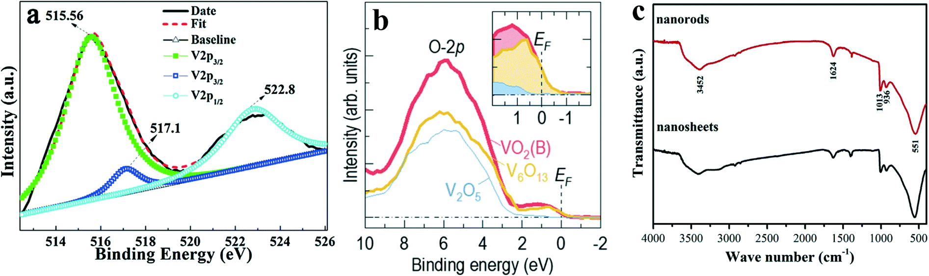 | ||
| Fig. 3 XPS of VO2(B): a) core-level spectra of V2p and O1s. Reproduced with permission.38 Copyright 2017, Applied Surface Science. b) X-ray photoemission spectroscopy near the Fermi energy (EF) was used to investigate the valence bands of VO2(B), V6O13, and V2O5. VO2(B) and V6O13 exhibit a significant spectral weight (enlarged in the inset) near EF, while V2O5 does not. Reproduced with permission.15 Copyright 2020, APL Materials. c) FTIR spectra of VO2(B) nanorods and nanosheets. Reproduced with permission.39 Copyright 2018, Electrochimica Acta. | ||
Fig. 3c shows the Fourier transform infrared (FTIR) spectrum of VO2(B). The absorption belonging to the vibration of V–O is mainly concentrated in the range of 400–1100 cm−1. Among the three absorption peaks of 540, 926 and 1047 cm−1, the strong absorption peak near 540 cm−1 corresponds to the bending of the V–O–V octahedron, and the absorption peak of 926 cm−1 is caused by the coupling vibration of V![[double bond, length as m-dash]](https://www.rsc.org/images/entities/char_e001.gif) O and V–O–V. Both of the above belong to the inherent properties of VO2(B). The cause of the weak absorption peak near 1047 cm−1 is more complicated. It is caused by the stretching vibration of the VO short bond, which involves vanadium ions in the oxidation state between V5+ and V4+. These vanadium ions easily cause partial interaction due to the large specific surface area of VO2(B) and O2 in the atmosphere.
O and V–O–V. Both of the above belong to the inherent properties of VO2(B). The cause of the weak absorption peak near 1047 cm−1 is more complicated. It is caused by the stretching vibration of the VO short bond, which involves vanadium ions in the oxidation state between V5+ and V4+. These vanadium ions easily cause partial interaction due to the large specific surface area of VO2(B) and O2 in the atmosphere.
3. Synthesis of VO2(B)
Since Théobald firstly discovered a new phase in vanadium dioxide in 1976,26 named VO2(B), the preparation of VO2(B) has always been an issue of great concern. The bulk crystal of VO2(B) is easy to fracture and can be converted to other phases owing to temperature changes.10,28 Moreover, different application scenarios require different VO2(B) with different microstructures. Therefore, a lot of effort has been made in the past to prepare VO2(B).24,40 Although obtaining pure VO2(B) is more challenging than the other phases of VO2,37,41,42 after decades of development, several methods for preparing VO2(B) have been realized, such as chemical vapor deposition (CVD), hydrothermal method, pulsed laser deposition (PLD), sol–gel method and magnetron sputtering.The above methods for preparing VO2(B) have their own characteristics. Some methods can produce films with high crystallinity, some methods can control the morphology of material growth, some methods can accurately control the proportions of different components, and some methods can be adapted to commercial processes. The above methods for preparing VO2(B) will be specifically introduced and compared to illustrate their respective advantages and disadvantages.
3.1. Chemical vapor deposition
CVD is widely studied and applied in industry because it can be used to prepare homogeneous films by precisely controlling the stoichiometric ratio, phase and morphology. As early as 1966, Takei et al.47 grew single crystal VO2 bulks by CVD. Generally speaking, CVD utilizes a gas precursor to react in a reaction chamber and deposit the reaction product on the substrate to form a thin film. The usual complete process of CVD is shown in Fig. 4a. In most cases, due to poor crystallinity and quality, the film deposited with a powder as a crystalline nucleus is not desirable.48 In 2017, Guo et al.49 of Shanghai University, China, utilized a simple CVD method, which does not require high vacuum to produce thermally sensitive VO2(B) films with suitable crystallinity, high uniformity and high performance at low cost. The vanadium(III)-2,4-pentanedionate (V(C5H7O2)3, 97%) precursor was heated at 150 °C for 2 h in the beginning and the injected high-purity argon flow rate (30, 50, 80, 120 standard cm3 min−1 (sccm)), substrate temperature (350, 375, 400, 450, 500 °C), and in situ annealing time (0, 1, 3, 5 h) were adjusted, and finally, the sample was taken out of the furnace below 50 °C. After the above process, VO2(B) films with different crystallinity and thermal sensitivity were prepared. In the experiment with controlled variables, the VO2(B) film at 375 °C (Fig. 5a) has the lowest vis-NIR transmittance, and the VO2(B) film at 30 sccm (Fig. 5b) and 1 h (Fig. 5c) has excellent TCR. These experiments have proved that the thermal sensitivity of the film annealed for 1 h at an argon flow rate of 30 sccm and a deposition temperature of 375 °C is relatively good, with a resistance of 11.27 kΩ, TCR of −2.87% K−1, suitable crystallinity and high uniformity, as shown in Fig. 5d. | ||
| Fig. 4 a) Schematic diagram of the CVD process: (1) precursor introduction; (2a) precursor absorbing; (2b) homogeneous reaction; (3) heterogeneous reaction; (4) film forming and coalescence; (5a), (5b) by-product transporting; (6) exhausting. Reproduced with permission.8 Copyright 2018, Applied Energy. b) Schematic representation of high-temperature autoclave. Reproduced with permission.43 Copyright 2020, Nanofabrication for Smart Nanosensor Applications. c) Schematic diagram of the PLD system. Reproduced with permission.44 Copyright 2018, Surface and Interface Analysis. d) Synthesis of various forms of materials by the versatile sol–gel process. Reproduced with permission.45 Copyright 2018, Curr. Sci. e) Schematic diagram of magnetron sputtering. Reproduced with permission.46 Copyright 2019, Heterogeneous Photocatalysis. | ||
 | ||
| Fig. 5 a) Transmittance spectra at 20 °C and 90 °C of the films that were deposited at different deposition temperatures for 2 h under 30 sccm. b) SEM images of the films that were prepared under different Ar gas flow rates at 400 °C for 2 h: 30 sccm; 50 sccm; 80 sccm; 120 sccm. c) Resistance–temperature curve of the films that were in situ annealed at 375 °C for 1 h and 3 h under 30 sccm. d) SEM image of the films that were in situ annealed at 375 °C for 1 h under 30 sccm. Reproduced with permission.49 Copyright 2017, Journal of Alloys and Compounds. | ||
In less than a year, the same team successfully utilized CVD to dope Mo or/and Al into the VO2(B) film.50 The method they chose was similar to that mentioned above. Molybdenum acetylacetonate ([CH3COCHC(O)CH3]2MoO2, 99%) or/and aluminum acetylacetonate (Al(C5H7O2)3, 99%) were employed so that Mo or/and Al was doped into the VO2(B) film. The SEM images of the final sample are shown in Fig. 6a. In general, there is no synergy between high conductivity and great TCR.51 According to the simulation results of first-principle calculations, Guo et al. found that if the co-doped elements meet two conditions – the radius is close to V and there is charge compensation, the lattice deformation of the doped VO2(B) film could be reduced. Fig. 6b shows the V L-edge and O K-edge X-ray absorption spectra (XAS) of the samples, and the results are tabulated in Fig. 6c. It can be found that the change about π* and σ* of the Mo–Al co-doped is the slightest in all the results, compared with undoped VO2(B). Thus, its film performance should be the best. The experimental results in Fig. 6d prove that the Mo–Al co-doped film has the best TCR, reaching −3.6% K−1. Therefore, the change in the lattice deformation in the VO2(B) film is the smallest when Mo and Al are co-doped. The ability to prepare uniform VO2(B) thin film and superior TCR make CVD a potential method for application in uncooled infrared detector.
 | ||
| Fig. 6 a) SEM images of the Mo–Al co-doped thin film. b) V L-edge and O K-edge XAS of undoped (sample I), Mo-doped (sample II), Al-doped (sample III) and Mo–Al co-doped (sample IV) VO2(B) thin films. c) V L-edge and O K-edge XAS fitting results of the four VO2(B) thin films. d) The differences between π* and σ*, square resistance and TCR values of the four VO2(B) thin films. reproduced with permission.50 Copyright 2018, Journal of Alloys and Compounds. | ||
3.2. Hydrothermal method
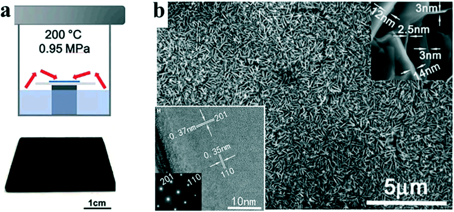
Broadly speaking, hydrothermal synthesis directly crystallizes materials from aqueous solutions by controlling the thermodynamic variables (temperature, pressure, composition, etc.).52 Nowadays, the hydrothermal method is closely linked with nanotechnology. Due to the highly controlled diffusivity in the strong solvent medium of the closed system, the hydrothermal method has special advantages for processing nanomaterials. Compared with traditional coarse-grained materials, the mechanical strength, diffusion coefficient, specific heat and resistivity of nanomaterials are higher.53 The core components for preparing the VO2(B) film using the hydrothermal method is the autoclave reactor, as shown in Fig. 4b.Recent studies have shown that the hydrothermal method has the advantages of low temperature (180–200 °C) preparation, friendly reaction environment, and ease of morphology and size distribution control. The autoclave facilitates the synthesis of VO2(B) nanostructures with a controllable shape.54 Many nanostructures have been successfully synthesized, including nanowires,55 nanobelts,56 nanorods,57 nanotubes,19 and 3D nanostructures.58,59 As shown in Fig. 7a, nanowires with a diameter of 50–60 nm and thickness of 6–10 nm were prepared by the reaction of V2O5, water and ethylene glycol.55 The ultra-thin wires deliver a higher capacity to store charge than the standard wires cycled under the same conditions (200 mAh g−1). Fig. 7b shows VO2(B) nanosheets with a thickness of several nanometers and width of tens of nanometer, which were obtained by the hydrothermal reaction between NH4VO3 and oxalic acid.57 As the cathode, the VO2(B) nanosheets exhibit better initial discharge capacity and cyclability than the VO2(B) bulk because of the high ability in overcoming the aggregation and stress to induce structural collapse of the sheet-like morphology. The stacked VO2(B) shown in Fig. 7c is a free-standing VO2(B) film formed by the hydrothermal reaction of V2O5, H2O2 and isopropyl alcohol on the plane (001) superposed by nanosheets.60Fig. 7d shows that using V2O5 as the vanadium source and glycerin as the reducing agent, VO2(B) nanobelts with the length of 1 μm and width of 50 nm with uniform morphology can be synthesized.56 It has been reported that hierarchical VO2(B) nanostructures are assembled from lower-dimensional nanostructures. For example, novel flowerlike VO2(B) micro-nanostructures assembled from single-crystalline nanosheets were prepared using PVP as a surfactant (Fig. 7e),58 and sea urchin-like VO2(B) nanostructures assembled from nanobelts were prepared by the hydrothermal method (Fig. 7f).59 This three-dimensional assembly can be promoted by increasing the concentration of the reducing agent and the reaction temperature. However, the high concentrations of the reducing agent may prevent VO2 from crystallizing, resulting in polycrystalline formation. In order to maintain the uniformity of the crystal form, the reaction temperature or reaction time should be increased. The ability to grow different nanostructures make the hydrothermal method a popular method in the field of VO2(B) preparation.
 | ||
| Fig. 7 a) TEM image of VO2(B) nanowire fabricated through hydrothermal synthesis. Reproduced with permission.55 Copyright 2008, Journal of Power Sources. b) TEM image of VO2(B) nanosheet fabricated through hydrothermal synthesis. Reproduced with permission.57 Copyright 2015, Journal of Materials Science & Technology. c) TEM image of stacked VO2(B) nanosheets fabricated through hydrothermal synthesis. Reproduced with permission.60 Copyright 2018, Materials Letters. d) TEM image of VO2(B) nanobelt fabricated through hydrothermal synthesis. Reproduced with permission.56 Copyright 2017, Journal of Nanoparticle Research. e) SEM image of nanosheet-assembled VO2(B) nanoflowers. Reproduced with permission.58 Copyright 2009, The Journal of Physical Chemistry C. f) SEM image of the nanobelt-assembled urchin-like VO2(B) nanostructure. Reproduced with permission.59 Copyright 2009, Inorg. Chem. | ||
Tian et al.61 of Chinese Academy of Inspection and Quarantine reported an ingenious preparation method based on the traditional hydrothermal method in 2019. The traditional hydrothermal method performs the oxidation–reduction reaction in a sealed and heated solution to generate VO2(B), while Zhang et al. transfer the reaction from inside the solution to a glass placed right above the solution, as shown in Fig. 8a. The solution is evaporated and redeposited on the glass to form the final product, which is called the hydrothermal evaporation method. After the reaction, the black product covers the surface of the glass plate. As shown in Fig. 8b, the black product is layered, uniform nanosheet of VO2(B), which is vertically distributed on the glass surface with a thickness in the range of 3–15 nm. The hydrothermal evaporation method overcomes the shortcoming of the hydrothermal method, i.e., difficulty of forming a uniform film with large area, thus greatly expanding its application range.
 | ||
| Fig. 8 (a) Schematic illustration of the synthesis of the metallic VO2(B) nanosheet array on glass and the prepared substrate covered with black VO2(B) nanosheets. (b) SEM images of the VO2(B) nanosheet arrays and the inset is the HRTEM image of the VO2(B) nanosheet, showing that the exposed crystal plane is (112). Reproduced with permission.61 Copyright 2019, iScience. | ||
3.3. Pulsed laser deposition
Pulsed laser deposition is one of the most commonly used physical vapor deposition processes. The schematic diagram of the PLD experimental device is shown in Fig. 4c. PLD technology began to develop in the late 1980s. In 1993, Borek et al.62 deposited directional grains of VO2 on a sapphire substrate for the first time. PLD, which is especially suitable for oxide growth, has developed rapidly in the field of film deposition in the recent years.VO2(B) thin film is usually prepared at low-temperature because the phase transition from VO2(B) to VO2(R) occurs after 400–450 °C.26,63 High quality thin films prepared by PLD normally required high temperature; thus, it was not until 2014 that PLD was used to prepare metastable VO2(B) thin films. Chen et al.64 took V2O5 as the target material to grow VO2(B) films on the SrTiO3 (STO) (001) substrate under the optimal substrate temperature of 550 °C and oxygen pressure of 10 mTorr. They found that the lattice matching between the film and the substrate was the main driving force for the preservation of the metastable phase. There are four possibilities for the growth of VO2(B) on SrTiO3 (STO) (001), as shown in Fig. 9b. Fig. 9d–f reveal the simulated diffraction patterns from different zones of VO2(B). The symmetric parallelograms (red solid and dashed lines) connect the diffraction patterns from [010] VO2(B) and [0![[1 with combining macron]](https://www.rsc.org/images/entities/char_0031_0304.gif) 0] VO2(B) zones, respectively. The symmetric squares (green dashed lines) connect the diffraction patterns from [100] VO2(B) or/and [00] VO2(B) zone axes, respectively. The small blue square corresponds to the substrate diffraction pattern.
0] VO2(B) zones, respectively. The symmetric squares (green dashed lines) connect the diffraction patterns from [100] VO2(B) or/and [00] VO2(B) zone axes, respectively. The small blue square corresponds to the substrate diffraction pattern.
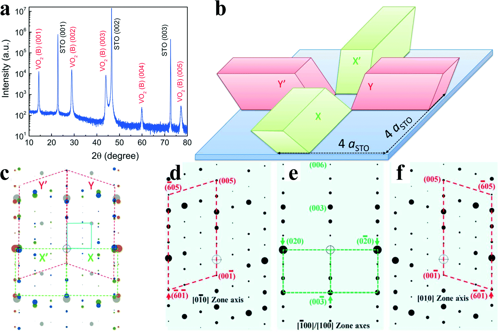 | ||
| Fig. 9 a) XRD θ–2θ scan of a 96 nm VO2(B) film directly grown on the STO (001) substrates. b) The matching diagram of VO2(B) in 4 possible variants on the STO substrate (coded as red and green corresponding to the simulated diffraction pattern in c). c) The combined simulated electron diffraction patterns from 4 different zones of the VO2(B) phase (red and green) and [010] zone of the STO substrate (blue). d)–f) The simulated electron diffraction patterns from 4 different zones of VO2 (B).64 Copyright 2014, Applied Physics Letters. | ||
The PLD method shows advantages such as low film pollution, fast growth rate and uniform orientation. It is possible to accurately control the growth conditions to obtain the phase, which researchers need. In 2015, Srivastava's team, National University of Singapore, controlled the laser frequency of PLD to control the rate at which vanadium reaches. They have grown monoclinic VO2(M), epitaxial tetragonal VO2(A) film and monoclinic VO2(B) film on the STO(100) substrate (Fig. 10a), as well as compared their structure and transportation. They investigated the effects of oxygen pressure and laser frequency on the stability of these crystal forms. The phase diagram of the different phases of VO2 was established (Fig. 10b). Their formation may be related to the distance between the V–V atoms caused by different oxygen pressures. At low oxygen pressures, the VO2(R) phase is preferred at the growth temperature, which subsequently return to the M phase (Fig. 10c) at room temperature due to the metal–insulator transition (MIT). When the oxygen pressure increases, the A phase with a longer average V–V distance (Fig. 10d) may be favored. Furthermore, by lowering the laser frequency to decrease the V arrival rate, the B phase with the longest V–V distance (Fig. 10e) is stabilized. Moreover, the symmetry of the phases could also be an important factor for their stabilization. The relatively more symmetric structure of VO2(A) over VO2(B) suggests VO2(A) to be more stable over a wide range of laser frequency.
 | ||
| Fig. 10 a) XRD θ–2θ patterns showing different phases for VO2 thin films. b) Phase diagram for different polymorphs of VO2 thin film grown by the PLD method. Reproduced with permission.28 Copyright 2015, APL Materials. The crystal structures of VO2 polymorphs, c) VO2(M), d) VO2(A) and e) VO2(B). Reproduced with permission.65 Copyright 2021, Nanomaterials. | ||
3.4. Sol–gel method
The sol–gel method refers to the material synthesis method that involves the preparation of a sol, then gelling it and removing the solvent. Fig. 4d shows the general sol–gel process. Turner summarized some advantages of the sol–gel method over the traditional process: good chemical homogeneity, large surface area, high chemical purity, and various forms of products.66In 2011, a team67 from the National Institute of Advanced Industrial Science and Technology in Japan obtained VO2(B) nanofibers (Fig. 11a) with high specific surface areas by simply annealing the aerogel in high vacuum, taking the aerogel of hydrated vanadium pentoxide (V2O5·xH2O) as the precursor. Since VO2(B) has the closest double-layer structure to the aerogel precursor, the conversion of the aerogel to VO2(B) can proceed smoothly with the lowest structural rearrangement resistance. Therefore, VO2(B) obtained by high vacuum annealing well inherits the unique structural characteristics of the aerogel precursor, such as high surface area, mesoporous network and nanofiber morphology. These unique structures leave more active sites and larger specific surface area in VO2(B), which is suitable as a cathode material for ion batteries. Fig. 11b shows that the discharge curve undergoes a rapid decline to 2.6 V, then a well-defined flat voltage plateau at 2.5 V, and finally a less-resolved second plateau at about 1.9 V, down to 1.5 V. They respectively correspond to the two intensive reduction peaks from the derived dQ/dV curves in Fig. 11c. The reduction branch and oxidation branch of the dQ/dV curve are in good symmetry, showing good reversibility of the electrode reaction. However, there is a problem in the above preparation process – its preparation cycle is too long, and the complete process requires nearly two weeks.
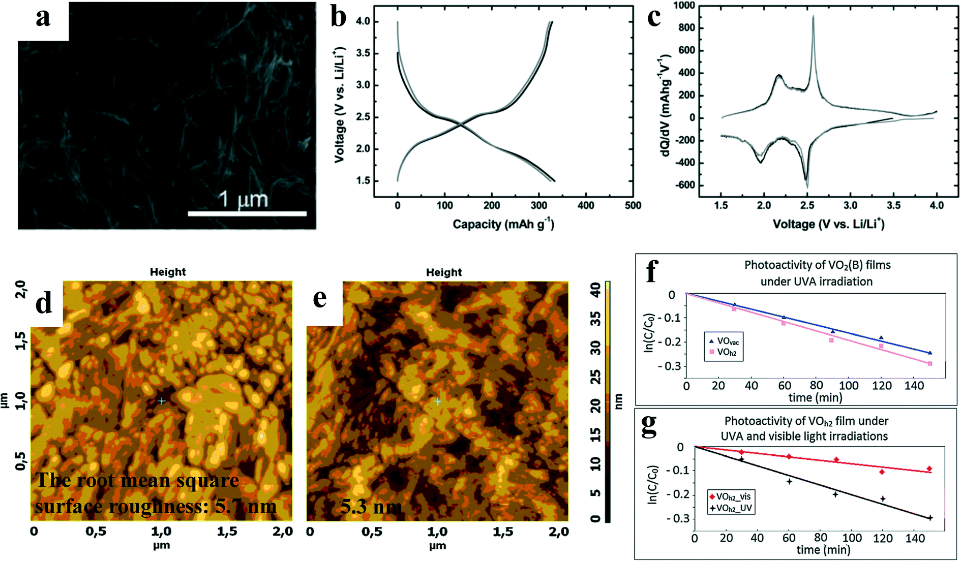 | ||
| Fig. 11 a) SEM images of VO2(B) obtained by annealing the aerogels at 400 °C for 10 h under high vacuum atmosphere. Discharge/charge curves and derived dQ/dV profiles of VO2(B) b) and c), the black and grey lines refer to the first and the second cycle, respectively. Reproduced with permission.67 Copyright 2011, Journal of Materials Chemistry. AFM pictures of d) VOh2 surface and e) VOvac surface. Photocatalytic activity of f) the VOh2 and VOvac samples, i.e., VO2(B), under UVA and g) VOh2 sample under both UVA and visible light irradiations. Reproduced with permission.68 Copyright 2014, Applied Surface Science. | ||
The VO2(B) film prepared by the sol–gel method by Monfort et al.68 from Comenius University overcame the problem of excessively long preparation time. V2O5 powder obtained by calcining 1 g ammonium metavanadate was dissolved in 100 mL of 15% H2O2 drop by drop, and V2O5 aqueous solution was synthesized. After all the powders were completely dissolved, the transparent orange solution containing oxo- and peroxyvanadate was heated to 70 °C, and the solution turned into a deep red gel. The V2O5·xH2O hydrogel was rotated at 60 revolutions per second (RPS) for 1 min and deposited on a clean Si/SiO2 and sapphire substrate. After deposition, the hydrogel was annealed at 400 °C for 10 min to dehydrate the film. Finally, it was annealed in a tubular oven. The whole process took no more than 12 h. As shown in Fig. 11d and e, the grain size of the film annealed in vacuum is smaller and more uniform than the film annealed in H2/Ar. It is because H2/Ar reacts with O2 in the film, resulting in more particles, more micro-cracks, and a thinner film. With these advantages, VO2(B) exhibits considerable photocatalytic activity in both UVA and visible light, as shown in Fig. 11f and g. It is worth thinking about enhancing its photocatalytic properties by doping it with another element or by increasing its surface area. Moreover, the report from Monfort et al. provides a detailed reference for the preparation of VO2(B) films by the sol–gel method, and the specific conditions and parameters can be designed according to the actual needs of VO2(B).
3.5. Magnetron sputtering
Fig. 4d shows the DC magnetron sputtering process. Usually, high-purity vanadium or vanadium oxide is the target, and the sputtering target is annealed to form a dense and uniform film. The magnetron sputtering method can deposit thin films at a low temperature with a high deposition speed. It is one of the mature thin film deposition techniques in the industry. Ding et al.69 proposed an effective strategy to modify the electronic properties of VO2(B) by inducing elastic strain through the TiO2(A) buffer layer in magnetron sputtering. Superior vis-NIR absorption (Fig. 12a) and high TCR (−3.48% K−1, Fig. 12b) was achieved. Investigation on the microscopic mechanism in Fig. 12c shows that tensile strain contributes to a reduction in the overlapping of the V-3d orbitals and an increase in the carrier concentrations along the c-axis in VO2(B). Fig. 12d shows that the larger the tensile stress applied to the sample, the more obvious increase in the conductivity was observed. Besides interfacial stress, the temperature rise causes additional tensile stress inside the material. Both improve the electrical conductivity and TCR values of VO2(B).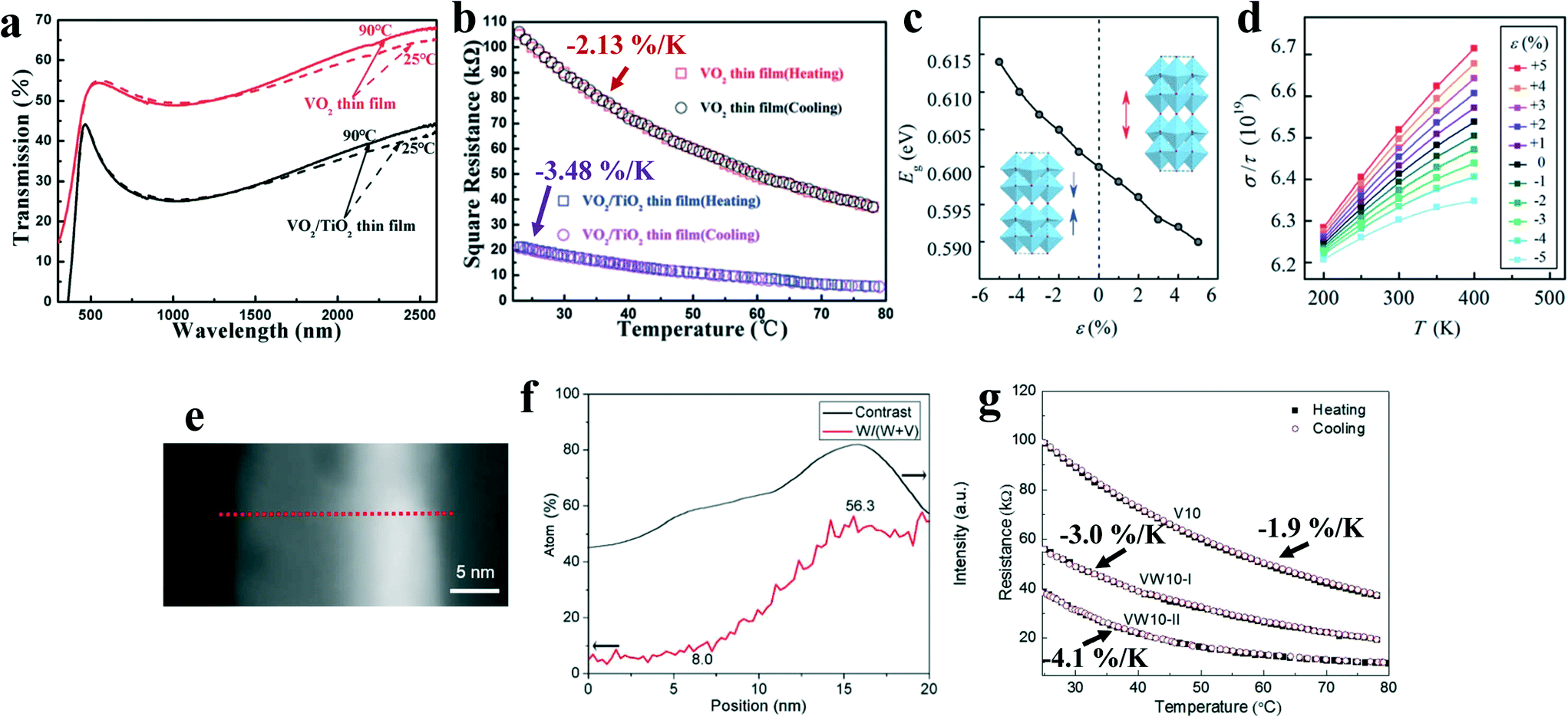 | ||
| Fig. 12 (a) Transmittance spectra at 25 °C and 90 °C for the as-prepared VO2 film, the VO2/TiO2 film deposited on quartz substrates, and the annealed films. (b) Resistance–temperature curves of the as-prepared VO2(B)/SiO2 thin film, and the as-prepared and annealed VO2(B)/TiO2 thin film. c) The ratio between the conductivity and relaxation time (σ/τ) of VO2(B) as a function of temperature under the strains ranging from −5% to 5% along the c-axis, σ/τ is given in 1019 (d). Reproduced with permission.69 Copyright 2017, RSC Advances. e) and f) EDS line-profiling and contrast from the red dotted line in the HAADF image of VW10-II. g) Temperature dependence of the square resistance curves for films V10 (undoped), VW10-I (W-doping layers) and VW10-II (graded thickness of W layers) under a total sputtering time of 10 min. Reproduced with permission.70 Copyright 2017, Journal of Advanced Ceramics. | ||
Zhang et al.70 successfully prepared a layered W-doped VO2(B) film by magnetron sputtering, which has better crystallinity and texture than the deposited film. It can be seen from Fig. 12e and f that the two-layer configuration of this 20 nm-thick film is formed by 12/8 nm-thick W-poor and W-rich layers, respectively. The inconspicuous boundary implies that there is a good mutual diffusion between W and VO2(B). Besides, 8 cat% W in VO2(B) strikes a good balance between a sufficient number of 3d electrons and the negative effect on the crystallinity by W substitution. As shown in Fig. 12g, the TCR of VW10-II is higher than that of undoped VW10 and VW10-I with larger thickness (30 nm) and obvious boundary due to larger grains with less grain-boundaries to generate lower site density of the defects in the bandgap. The above result shows that the doping can tailor the multi-layered microstructure to optimize the performance of the VO2(B) films, as well as affects the crystallinity of the VO2(B) phase and its degree of texture.
3.6. Comparison of various preparation methods for VO2(B)
The five mainstream methods for preparing VO2(B) have been introduced above. It can be found that most of these methods convert V in the vanadium source into V of +4 via an oxidation–reduction reaction. The commonly used vanadium source is V2O5. During the formation process, VO2(B) needs an oxygen-rich environment.71 It could be found that the main factors affecting the morphology, particle size, microscopic morphology and performance of the VO2(B) products are concentrated in the reaction atmosphere, reducing agent concentration, reaction temperature and time.Table 4 summarizes the above methods for preparing VO2(B), listing the advantages and disadvantages of each method. At present, most of studies on VO2(B) is carried out in the form of nanomaterials. Hydrothermal and sol–gel methods are simple and more suitable for growing nanomaterials with different types of nanostructures. They are more popular to prepare VO2(B) with a finely adjustable nanostructure for application as metal ion battery electrode. CVD, PLD and magnetron sputtering are more suitable to prepare thin film samples with high quality. In particular, magnetron sputtering is one of the most widely applied thin film deposition technologies in the industrial field, which can obtain uniform thin films with a large area. Therefore, VO2(B) prepared by magnetron sputtering could quickly integrate into the industrial production process. These methods are more suitable for application in semiconductor devices, for example, uncooled infrared detectors. Last but not least, researchers should choose a suitable method to prepare according to the actual situation so that the obtained VO2(B) product could meet the final requirement.
| Method | Raw material(s) | Atmosphere | Production | Application | Reaction condition | Advantage | Disadvantage | Ref. |
|---|---|---|---|---|---|---|---|---|
| CVD | Vanadium(III) acetylacetonate, | 99.99% argon | VO2(B) thin films | Uncooled IR detectors | 150 °C, 2 h;Flow rate: 30 sccm; Substrate temperature: 375 °C |
• Could be doped | • Complex preparation process | 49 |
| • Preparation of composite materials | • Poor film-substrate adhesion | |||||||
| • Template-assisted growth | ||||||||
| Vanadium(III) acetylacetonate, Mo acetylacetonate, Al acetylacetonate | 99.99% argon | Mo–Al co-doped VO2(B) thin films | Uncooled IR detectors | 170 °C, 75 min;Flow rate: 30 sccm; Substrate temperature: 400 °C, 75 min |
50 | |||
| Hydrothermal method | V2O5, sucrose, distilled water | 50 mL autoclave | Carbon-coated VO2(B) nanobelts | Cathode of lithium-ion batteries | 180 °C, 24 h | • Simple reaction conditions | • High pressure | 54 |
| • Several products could be prepared | • Poor film-substrate adhesion | |||||||
| V2O5, citric acid, oxalic acid, ethylene glycol, surfactants | A Teflon-lined stainless-steel autoclave | VO2(B) nanoparticles | Gas sensors | 160–180 °C, 6–10 h | • High purity and good crystal form | 72 | ||
| V2O5 powders, H2O2, isopropanol, deionized water | Autoclave | Free-standing VO2(B) thin films | Uncooled IR detectors | 180 °C, 5 h | • Adjustable product morphology | 60 | ||
| PLD | Vanadium metal target | Oxygen and argon atmosphere (70 mTorr) | VO2(B) thin films | Infrared sensors | 375–425 °C;Flow rate: 10 sccm Ar, 15 sccm O2; | • Less pollution to the film | • Unable to prepare large area film | 73 |
| • Fast growth rate | ||||||||
| • Highly orientated | ||||||||
| V2O5 target | Oxygen pressure of 10 mTorr | VO2(B) thin films on SrTiO3 substrates | VO2(B) based battery | Substrate temperature: 550 °C | • Suitable for multi-component compound deposition | • Low target utilization | 64 | |
| • Phase controllable | • Expensive | |||||||
| Sol–gel method | Vanadyl triisopropoxide, alkoxide, acetone solution, deionized water, | Vacuum atmosphere (10−2 Pa) | Nanocrystalline VO2(B) | Lithium-ion batteries | 250 °C, 4 h;400 °C, 10 h | • Simple reaction conditions | • Uneven distribution of pores | 67 |
| • Controllable product valence | • Most reactions take longer | |||||||
| • Good uniformity | ||||||||
| Ammonium metavanadate, hydrogen peroxide | Vacuum or 5% H2/Ar atmosphere | VO2(B) films | Photocatalysis | 625 °C or 500 °C, 30 min | • High porosity and large specific surface area | 68 | ||
| • Adjustable particle size | ||||||||
| Magnetron sputtering | TiO2 and VO2 targets | Vacuum atmosphere (1 Pa);TiO2 layers: O2 (99.99%) and Ar (99.99%) gas mixture (1.0% O2 content); VO2 layers: pure Ar gas |
VO2(B) thin films with TiO2(A) buffer layer | Uncooled IR detectors | 30 sccm;TiO2 layers: radio frequency (RF) power of 160 W for 1200 s, annealing at 450 °C for 2 h in Ar atmosphere; VO2 layers: RF power of 200 W for 900 s, annealing at >350 °C for 2 h in Ar atmosphere |
• Fast deposition | • Low target utilization | 69 |
| • Low substrate temperature | ||||||||
| • Little damage to the film | • Expensive | |||||||
| • High purity, good density and uniformity | ||||||||
| • High repeatability, easy to industrialize | ||||||||
| V and W metal target | Vacuum atmosphere (0.7 Pa); VO2 layers: O2 (99.99%) and Ar (99.99%) gas mixture (2.5% O2 content); W-doping layers: Ar gas | VO2(B) thin film with layered W-doping | Uncooled IR detectors | 30 sccm;Annealing at 450 °C for 2 h in Ar atmosphere |
70 |
4. Application of VO2(B)
The most popular and widely reported applications of VO2(B) are metal ion batteries and uncooled infrared detectors. VO2(B) shows large interlayer space (8.2 Å along the b-axis20), and its nanostructure with a large specific surface area can also provide more active sites as the diffusion channel for the rapid intercalation and de-intercalation of ions in reversible lithium-ion batteries.22,23 In addition, VO2(B) also has the advantages of proper electrode potential and excellent lattice shear resistance74 during the charging cycles. They are exactly what metal ion batteries need. Therefore, VO2(B) is a promising cathode material in lithium-ion batteries.75The material requirements for the new generation of uncooled infrared detectors mainly focus on two aspects: increasing the temperature coefficient of resistance (TCR) value and reducing the noise level. Compared with VO2(M)76 with insulator–metal phase transition characteristics, V2O577 with high resistivity and high noise level, and VOx with TCR affected by vacancies, VO2(B) shows no phase transition around the room temperature. It is thermal hysteresis and 1/f noise is low, while TCR is high with suitable resistance, which is suitable for thermal sensors in uncooled infrared detectors.
4.1. Cathode for metal ion batteries
Metal ion batteries have broad application prospects in large-scale energy storage systems.78,79 Various metal ion batteries, including lithium-ion batteries,23 aluminum-ion batteries,80 zinc-ion batteries,11 and magnesium-ion batteries,39 have requirements for cathode materials focused on the following points: capacity, rate ability, energy density, power density, and cycling performance. The capacity, rate capability, and cycle performance are obtained by fitting the experimental data, while the energy density and power density are obtained by calculation. The calculation formulas are as follows. | (1) |
 | (2) |
As we all know, VO2(B) is constructed from irregular VO6 octahedra, which share corners and edges to form a tunnel-like frame. The tunnel structure is conducive for the rapid intercalation and deintercalation of partial metal cations in VO2(B). The diffusion time (t) of ions is proportional to the square of the diffusion length (L): t ≈ L2/D (D is the diffusion coefficient);81 thus, reducing the feature size of the material is beneficial for shortening the diffusion time of ions. Therefore, when used in metal ion battery cathode material, VO2(B) usually appears in the form of nanomaterials.
The charge–discharge cycle in water-based Zn2+ battery: insertion of metal cations: as shown in Fig. 13a and b, when the Zn2+ battery is discharged, Zn2+ is gradually inserted into the interlayer tunnel, which is parallel to the b or c axes.22 At this point, the lattice spacing of the (−601), (020), and (−404) planes in VO2(B) will increase slightly, with d−601 = 0.202 + 0.011 nm, d020 = 0.185 + 0.008 nm, and d−404 = 0.156 + 0.003 nm, respectively. The extraction of metal cations: when the Zn2+ battery is charged, Zn2+ is gradually extracted from the interlayer tunnel, and the lattice spacing of the (−601), (020) and (−404) planes will reversibly restore to the initial position.
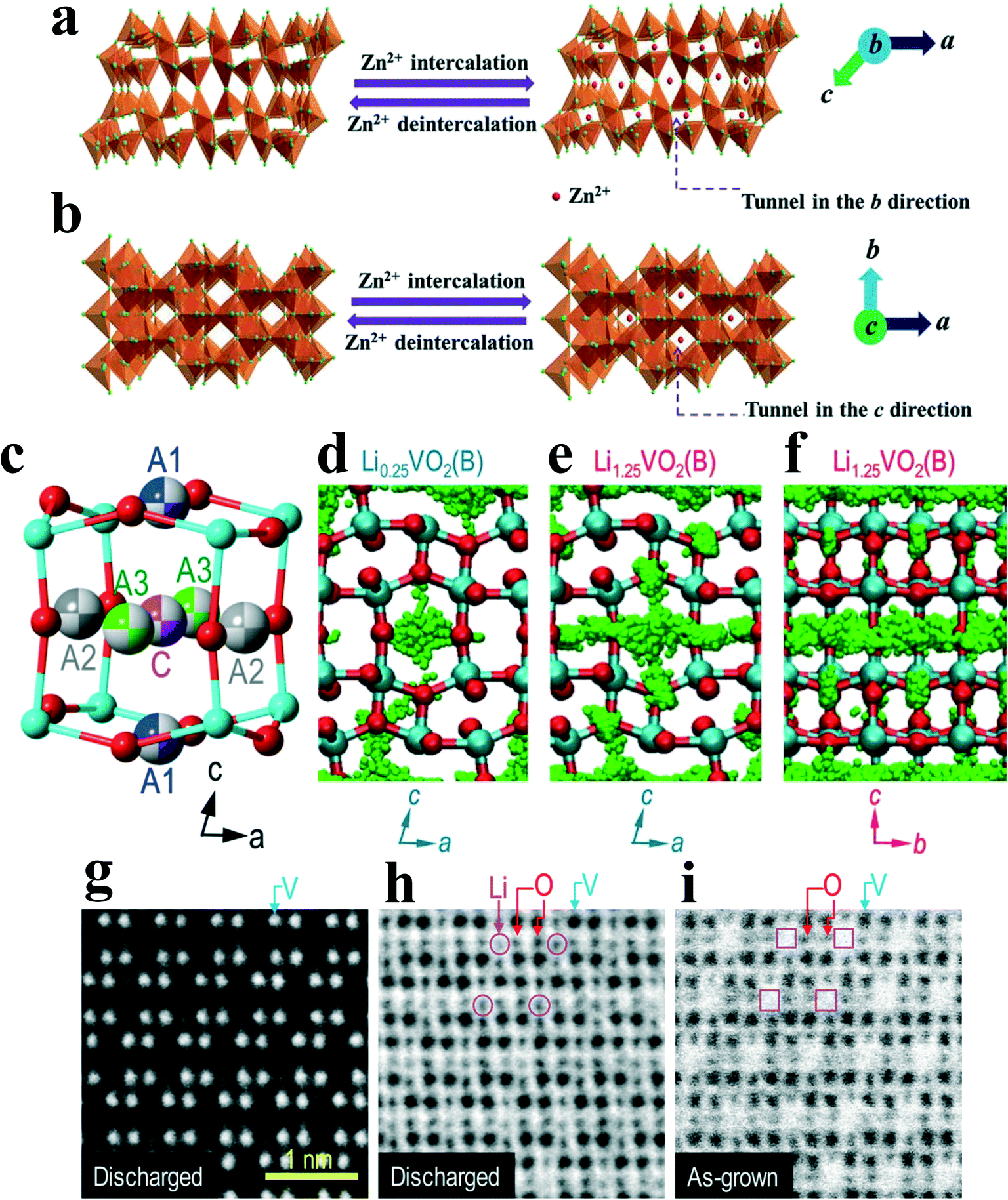 | ||
| Fig. 13 Schematic view of Zn2+ intercalation/deintercalation VO2(B) nanofibers projected along the direction of the a) b and b) c axes, respectively.22 Reproduced with permission.82 Copyright 2013, Adv. Mater. c) Schematic of Li ion adsorption sites in VO2(B). There are four possible adsorption sites: C, A1, A2, and A3. d) Li ion distribution in Li0.25VO2(B). C is the most preferred Li adsorption site, while A1 and A2 sites have non-negligible probability density. e) Li ion distribution in Li1.25VO2(B) (maximum theoretically modeled concentration), showing increased ion hopping to the A1 sites. f) Significant diffusion of Li ions is observed along the b-axis in Li1.25VO2(B). Cross-sectional HAADF g) and ABF STEM images h) of a discharged VO2(B) film, which clearly indicate the projection of one-dimensional channels. i) An ABF-STEM image of an as-grown VO2(B) film is shown comparatively. No evidence of Li was seen in the as-grown VO2(B) sample, clearly confirming that the dark contrast in discharged VO2(B) shown in panel g is caused by Li intercalation. Reproduced with permission.13 Copyright 2017, Nano Letters. | ||
In addition to interlayer intercalation/deintercalation behavior, Li+ also follow diffusion dynamics and preferential pathways.13Fig. 13c and d show the distribution of Li+ (green symbols) at a small concentration of Li (x = 0.25 in LixVO2(B)). Li+ are mainly found at the center of the cage, i.e., the C site, which is the most stable Li adsorption site. In addition, there is a non-negligible probability to find Li+ at A1 and A2. When the Li+ concentration increases up to the maximum theoretically modeled value (x = 1.25), more accumulation of Li+ at A sites, especially A1, is observed (Fig. 13e and f). This result suggests that the relative site adsorption energies could vary with the Li+ concentration. Overall, most Li+ ions are found to diffuse along the b-axis, as expected due to the large open channel space (Fig. 13f), while the diffusion along the a-axis also becomes significant when the Li concentration is increased, as shown in Fig. 13e. Fig. 13g–i proves the correctness of the simulation results. Though only the heavy atom V shows a bright contrast in the HAADF image (Fig. 13g), it is able to visualize other light atoms including O and Li atoms by ABF imaging (Fig. 13h). Even after 200 charging/discharging cycles, there is no structural distortion in the discharged VO2(B).
The pure layered nanobelt structure (Fig. 14a) allows metal cations to intercalate between the layers. However, the traditional structure will produce unavoidable volume expansion when metal cations are intercalated, resulting in strains that cannot be released in time. At this point, nanobelts tend to accumulate during the circulation process, and accumulation will hinder the circulation. If the structure is converted to a hybrid VO2(B) nanostructure (Fig. 14b), it could provide rapid strain relaxation for the expansion of metal cations during the intercalation–deintercalation process, increase the effective electrode–electrolyte contact area, and shorten the ion's diffusion path. The lattice strain can also be adjusted along the c-axis (the direction of the co-angular VO6 octahedron).32 The electron sharing along the [001] direction (c-axis) between the vanadium atoms may lead to stronger correlation effects between the electrons, which affects the electronic properties of VO2(B).69 As shown in Fig. 14c and d, compared to pure nanobelt, the hybrid nanostructure VO2(B) cathode has better charge/discharge and cycle performance.
 | ||
| Fig. 14 a) The hybrid nanostructure provides facile strain relaxation for swelling during lithiation/delithiation, and effective electrode-electrolyte contact area to shorten the ion diffusion pathway. b) In the pure nanobelt structure, the strain could not release completely or promptly. The nanobelts tend to aggregate during cycles, leading to poor cycling performance. c) Cycling performance of the hybrid nanostructural (HNS) and pure nanobelt (PNB) VO2(B) cathodes cycled at 100 mA g−1 in 2–3 V, and the corresponding coulombic efficiency. d) Rate performance at various current densities from 20 to 2000 mA g−1. Reproduced with permission.82 Copyright 2013, Adv. Mater. | ||
In the case of lithium ions storage, VO2(B)/graphene ribbons prepared by Yang et al.83 exhibit a high diffusion coefficient of ≈10−10 cm2 s−1, leading to an ultrafast rate ability of 204 mAh g−1 at 37.2 A g−1. One reason why VO2(B) prepared by Yang et al. through the hydrothermal method can maintain a good rate during rapid discharge is that VO2(B) is a nanomaterial. Another reason is that the radius of Li+ is small (0.76 Å). Even when storing the large-sized sodium ions, VO2(B) is still able to tolerate the high current rates up to 93 mAh g−1 at 36 A g−1.84 Chao et al. designed VO2(B)@GQD (graphene quantum dots), which is a cathode material for sodium ion battery, with extremely high cycle stability. After 1500 cycles at 18 A g−1, its capacity remained at 88%.
As for magnesium ion, which has a slightly smaller ionic radius than sodium ion, the performance of VO2(B) is not satisfactory. When the pure VO2(B) nanorods prepared by Luo et al.39 were used as the cathodes of magnesium ion batteries, although they have good capacity and rate capabilities, the cycle performance was indeed poor. This may be due to the fact that only part of the V3+ (belonging to V2p1/2) of vanadium oxide participates in the re-oxidation after losing magnesium during Mg2+ intercalation and deintercalation in the VO2(B) nanorods, resulting in the degradation of the VO2(B) performance. Therefore, when Cai et al.86 took VO2(B) as the cathode material of aluminum-ion batteries, the solution environment was changed to acidic because H+ and Al3+ participated in the intercalation and deintercalation, which would reduce the volume change of VO2(B) caused by intercalation and deintercalation.
Zinc ion batteries (ZIB) may have a larger ionic radius in metal ion batteries. Because VO2(B) nanofibers possess unique tunnel transport pathways and little structural change on Zn2+ intercalation, the limitation from solid-state diffusion in the vanadium dioxide electrode is eliminated. Thus, it can still play an important role in ZIB. The nanofibers prepared by Ding et al.22 have a maximum capacity of 357 mAh g−1, a rate capability of 171 mAh g−1 at 51.2 A g−1, and a capacity retention rate of 91.2% of the initial capacity (274.1 mAh g−1) after 300 cycles. If VO2(B) is combined with a suitable material to make a composite material, its performance can be further improved. Cui et al.11 reported their results in 2020. As shown in Fig. 15, the combination of VO2(B) and reduced graphene oxide (RGO) improved the performance to a higher level – the highest capacity of 456 mAh g−1, a rate capability of 292 mAh g−1 at 10 A g−1, and a capacity retention rate of 94.6% after 600 cycles. They also listed the comparison of the energy density of the current zinc-ion battery cathode materials (Fig. 15b).
 | ||
| Fig. 15 a) Schematic diagram of ZIB. b) Ragone plot based on the total mass of the whole electrode, and other reported materials for aqueous ZIBs. c) Cycling performances of VO2 and VO2/RGO at current densities of 0.2 and 5 A g−1, respectively. Reproduced with permission.11 Copyright 2020, Chemical Engineering Journal. | ||
Table 5 summarizes the performance reports of VO2(B) as metal ion battery cathode materials in the recent years. At present, the hydrothermal method has become the most popular preparation method by virtue of its advantages in controlling the structural details of VO2(B). One can say that the research progress of VO2(B) in this field in the past 10 years is encouraging, and the experimental results have gradually approached that of practical products. In particular, the VO2(B) base composite is considered as a better choice to improve the performance, reduce the costs, and make up for the shortcomings. The change in the thinking is more suitable for promoting the research and development of materials.
| Ion battery type/VO2(B) type | Preparation method | Capacity (mAh g−1) | Rate ability (x mAh g−1 at y A g−1) | Energy density/power density (Wh kg−1/W kg−1) | Cycling performance | Ref. |
|---|---|---|---|---|---|---|
| Li+/VO2(B)/graphene ribbons | Hydrothermal method | 410 | 204 at 37.2 | — | 90% after 1000 cycles | 83 |
| Li+/VO2(B)@C(6.6 wt%) | Hydrothermal method | 128 | 100 at 2 | — | — | 54 |
| Li+/VO2(B) | Sol–gel method | — | 410 at 0.208 | — | — | 67 |
| Na+/VO2(B)@GQD | Hydrothermal method | 421 | 93 at 36 | 100/42 | 88% after 1500 cycles | 84 |
| Mg2+/VO2(B) nanorod | Hydrothermal method | 394 | 240 at 0.1 | — | 52.2% after 60 cycles | 39 |
| Al3+/VO2(B) nanobelts | Hydrothermal method | — | 234 at 0.15 | 134/70 | 77.2% after 1000 cycles | 86 |
| Zn2+/VO2(B) nanofibers | Hydrothermal method | 357 | 171 at 51.2 | 297/180 | 91.2% after 300 cycles | 22 |
| Zn2+/VO2(B)/RGO | Hydrothermal method | 456 | 292 at 10 | 317/70 | 94.6% after 600 cycles | 11 |
| Flexible battery/CFC@VO2(B) | Hydrothermal method | 145 | 91 at 2 | — | 90% after 200 cycles | 85 |
4.2. Uncooled infrared detectors
Infrared detectors are widely applied in different fields including military, security, housing construction, transportation, and household appliances, with huge market demands and sufficient development potentials. At present, infrared detectors have gotten rid of the limitations of large-scale refrigeration equipment and are booming in uncooled infrared detectors.87 The microbolometer is the key pixel detector in the uncooled thermal imaging system.88 The main advantage of the microbolometer technology is that it can work at room temperature and its response band is wide enough from infrared to millimeter wavelengths.49 At room temperature, VO2(B) has the characteristics of low 1/f noise, suitable resistivity and high TCR, which is very suitable for microbolometers. As early as 1998, Wada et al.89 used VO2(B) film as the thermally sensitive material to produce a 256 × 256 bolometer-type uncooled infrared detector, and finally obtained thermal images with a noise equivalent temperature difference of 0.15 K.The key parameter for a bolometer material is the TCR that quantifies the change in the resistance as a function of a given temperature change.
 | (3) |
 | (4) |
 | (5) |
The preparation of vanadium oxide films with suitable sheet resistance (R0) and high TCR is the basis for the preparation of high-performance microbolometers.91 Ding et al.69 prepared a VO2(B) film with a TCR of −2.13% K−1 and a resistance of 94.0 kΩ by magnetron sputtering; Guo et al.49 prepared a VO2(B) film with a TCR of −2.89% K−1 and a resistance of 37.3 kΩ by CVD; Gao et al.60 prepared a VO2(B) film with a TCR of −3.0% K−1 by the hydrothermal method. The above reports show that the potential of VO2(B) is sufficient, and the potential contained in VO2(B) can be realized by improving the preparation process.
Table 6 is a summary of TCR and resistance of VO2(B) thin film that shows potential in a bolometer. Through comparison, it can be clearly found that VO2(B) doping (W doping,70 Mo–Al co-doping50) or making VO2(B) have a synergistic effect with other materials (RGO,16 TiO2(A),69 graphene14) can well improve its thermal performance. The higher the TCR, the more finely VO2(B) monitors the temperature changes and the suitable resistance can effectively suppress the 1/f noise and improve the detection rate.
| VO2(B) type | Preparation method | TCR (% K−1) | R 0 (kΩ) | τ (s) | Ref. |
|---|---|---|---|---|---|
| W-doped VO2(B) film | Magnetron sputtering | −4.1 | 33.3 | — | 70 |
| RGO/VO2(B) | Sol–gel method | −2.78 | 21.22 | — | 16 |
| Mo–Al co-doped VO2(B) | CVD | −3.6 | 16.2 | — | 50 |
| VO2(B) film | Hydrothermal method | −3.0 | — | — | 60 |
| VO2(B) film | CVD | −2.89 | 37.3 | — | 49 |
| VO2(B)/TiO2(A) | Magnetron sputtering | −3.48 | 18.97 | — | 69 |
| Graphene nanowalls/VO2(B) | CVD | −3.2 | 12.98 | — | 14 |
| VO2(B) NRs | Hydrothermal method | — | — | 0.96 (vacuum)0.48 (air) | 92 |
Recently, VO2(B) has been reported to be integrated into the pipeline process of uncooled infrared detectors. Lee et al.93 have fabricated highly textured and thermally stable VO2(B) thin films on an amorphous SrTiO3 layer using a reactive sputtering technique. The schematic fabrication process, which conforms to the standard industrialization process, is shown in Fig. 16a. It is also worth mentioning that the fabrication process used is suitable for application to monolithic infrared detectors since all fabrication processes are carried out at temperatures lower than 350 °C. The sensor arrays consist of microbolometers with a single active pixel area of 24 × 26 μm2 (Fig. 16b). Fig. 16c shows that the resistivity and TCR values at 100 °C were quite stable for a month at about 8.40 × 10⁻² Ω cm and 1.24% K−1, respectively, and there was no significant change in the resistivity and TCR value at this temperature. This shows the high thermal stability of the VO2(B) film and indicates the feasibility of long-term, stable, high-temperature operation of the microbolometer without a thermoelectric cooler, which are highly encouraging to those seeking cooler-free microbolometer image sensors operating at high temperature.
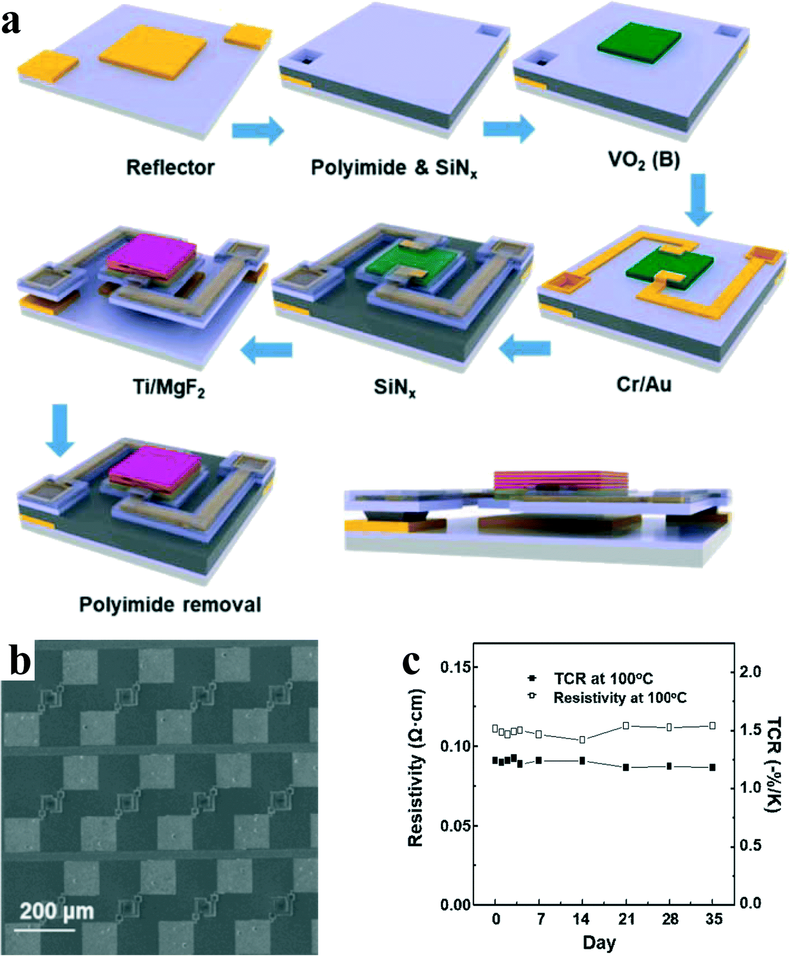 | ||
| Fig. 16 a) Schematic images of the fabrication process of the microbolometer with an IR absorber. b) Scanning electron micrograph top views of the microbolometer with an IR absorber. c) Resistivity and TCR change over 35 days at 100 °C. Reproduced with permission.93 Copyright 2021, Applied Surface Science. | ||
VO2(B) also shows good response performance from ultraviolet (UV) to NIR (Fig. 5a).15,29,49,50,69 It is because of the excitation from the V 3d band to the conduction band.15,28,30 The photoresponsive mechanism of VO2(B) in UV-NIR region includes the generation of free carriers and their subsequent transport. The surface state from surface defects, vacancies and dangling bonds will affect the generation and transport of free carriers. It has been reported that VO2(B) is susceptible to the influence of O2 and humidity in the atmosphere, thereby partially changing its electrical properties. The interaction between VO2(B) and O2 can be divided into two steps: the adsorption and desorption of oxygen molecules, as shown in Fig. 17a.92
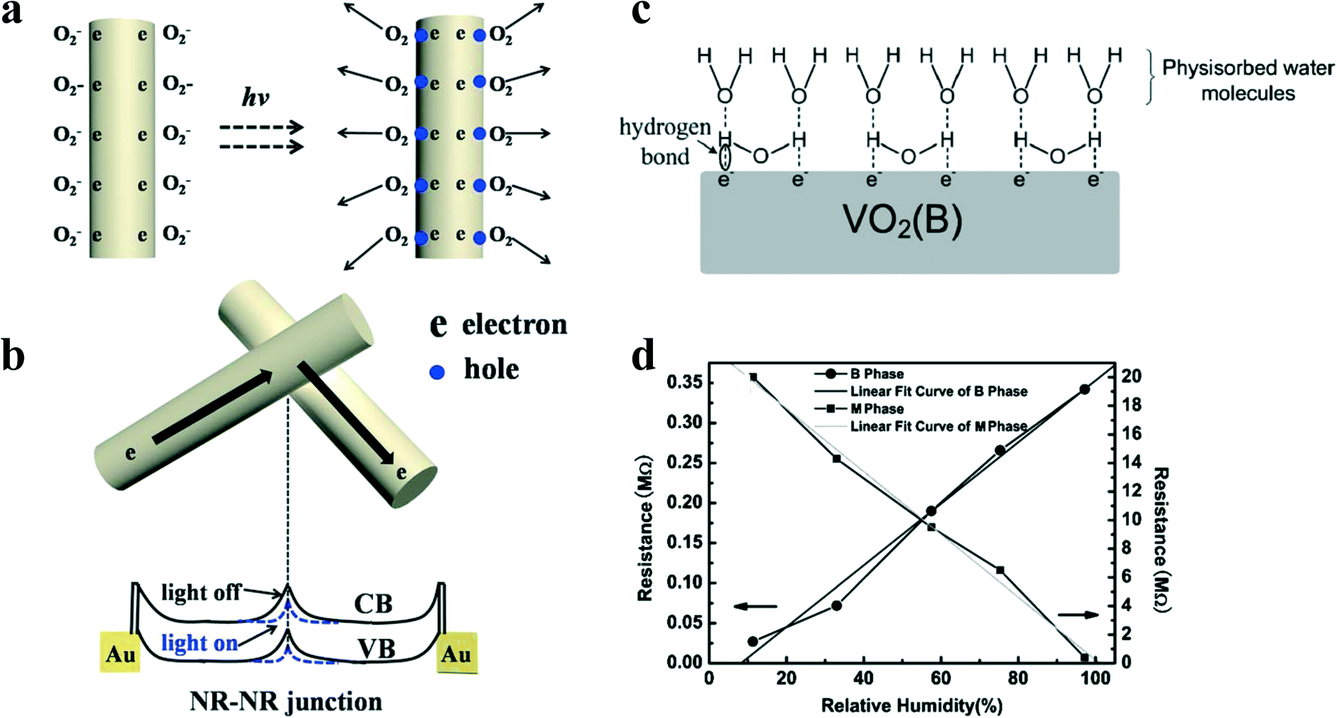 | ||
| Fig. 17 Schematic illustration of a) oxygen adsorption in the dark and oxygen desorption upon illumination of the nanorods; b) NR–NR junction barrier for electron transport and its change upon illumination. The solid line denotes “light off”, and the dashed line denotes “light on”. Reproduced with permission.92 Copyright 2017, Applied Physics Letters. c) Schematic diagram of the combination between VO2(B) and H2O. d) Relative humidity vs. DC resistance plots at 25 °C for VO2(B) and VO2(M) nanoflowers. The correlation coefficients of the B phase curve and of the M phase curve are 0.9939 and −0.9968, respectively. Reproduced with permission.18 Copyright 2011, Electroanalysis. | ||
| O2(gas) → O2(ads) | (6) |
| O2(gas) + e− → O−2(ads) | (7) |
This adsorption–desorption mechanism, as shown in Fig. 17a, increases the number of unpaired electrons and reduces the width of the depletion layer, resulting in a significant photocurrent enhancement. In addition, the junction barrier between the VO2(B) nanorods has an impact on electron transport. The resistance of the two nanoparticles in contact is primarily determined by the junction barrier between them rather than by their inherent resistance since the junction barrier creates significant band bending near the surface of the nanoparticle, through which the carrier needs to pass. In the developed photodetectors, electrons tunnel from one nanoparticle to another, while the junction barrier between the two must be overcome (Fig. 17b).
Apart from oxygen molecules, the influence of water molecules in air on the electrical properties of VO2(B) cannot be ignored. In general, water molecules can be adsorbed by physical or chemical means. For VO2(B), the main charge carrier is electrons. Under high humidity, due to the polarity of water molecules, some of the electrons will electrostatically combine with the positively charged hydrogen of the water molecules to form hydrogen bonds (Fig. 17c). Therefore, the density of free electrons on the surface of VO2(B) shows a downward trend during the adsorption process, resulting in an increase in the resistance with increasing humidity, as shown in Fig. 17d. The hydrogen bond is not as strong as the covalent bond formed during the chemical adsorption of H2O by VO2(M). Therefore, as the environmental humidity changes, the charge density does not change much so that the resistance of VO2(B) decreases less than that of VO2(M).18
4.3. Gas sensors
In terms of humidity sensors, few people regarded VO2(B) as sensing materials before 2010. It was not until Yin et al.18 found that VO2(B) had higher sensitivity than the other semiconductor oxide humidity sensors under low humidity; Zhu et al.72 found that VO2(B) nanoparticles had good sensitivity to alcohols (ethanol, isopropanol, butanol) and acetone that VO2(B) in humidity/gas sensors was gradually carried out. However, the gas sensor based on VO2(B) is far from being systematically studied in terms of its mechanism, which makes its development lacking of theoretical guidance. Related reports on the gas response of VO2(B) have gradually appeared in the recent years.In addition to the effects of water molecule adsorption mentioned above (Fig. 17c), different gas molecules act in different ways. The most stable adsorption configurations of gases on Au–VO2 are shown in Fig. 18a–d. The bonds lengths of H–H, C–H, C–O and C–O in H2, CH4, CO and CO2 molecules are 0.74, 1.14, 1.51 and 1.51 Å, respectively. CH4-adsorbed Au–VO2 system shows the smallest adsorption distances, which is related to the strong sensing characteristics of Au–VO2 toward CH4 gas, and consists of experimental observation.94 The above results were obtained by Joy et al.95 through density functional theory and molecular dynamics studies. They speculated that H2, CO, and CO2 are related to physical adsorption, and CH4 corresponds to chemical adsorption.
 | ||
| Fig. 18 The stable adsorption configurations for a) H2, b) CH4, c) CO and d) CO2 on Au–VO2. Reproduced with permission.95 Copyright 2020, Physics Letters A. e) Liquified petroleum gas sensing model for the VO2 nanorod sensor. Reproduced with permission.96 Copyright 2015, Nanoscale. f) SEM images of the VO2(B) ultrathin vertical nanosheet array prepared at oxalic acid concentrations of 0.14 mol L−1. g) Schematic diagram of the grain boundary barrier model. Reproduced with permission.97 Copyright 2021, ACS Appl Mater Interfaces. | ||
For this chemical adsorption mechanism, Dey et al.96 extended their scope of action to liquefied petroleum gas (LPG). The entire mechanism is illustrated pictorially through Fig. 18e. When the flow of LPG is stopped for recovery, the oxygen molecules in air will be adsorbed on the film, and the capture of electrons through the processes indicated in eqn (6) and (7) will increase the sensor resistance and the initial conditions get restored and the cycling reaction continues. Because the sensing mechanism is based on the chemisorption reaction that takes place at the surface of the metal oxide, increasing the specific surface area of the sensitive material leads to more sites for the adsorption of gases.
In addition to the influence of the adsorption mechanism, the nanostructure of VO2(B) also affects the sensitivity of the gas sensors. Liang et al.97 prepared VO2(B) ultrathin vertical nanosheet array using a hydrothermal method. They used density functional theory to analyze the adsorption of NO2 on the surface of VO2(B) and found that when the thickness of nanosheets is much larger than 2λD (λD is the Debye length of about 10 nm), a large part of the nanosheet interior cannot interact with the gas. As shown in Fig. 18f, when the thickness of the nanosheet is close to 2λD, the space charge layer completely occupies the conductive path. At this time, the resistance of the conductive path is almost completely controlled by the space charge layer, and the gas response reaches the highest. Moreover, when the VO2(B) nanosheets contact each other, the energy band at the grain boundary bends to form a homojunction potential barrier. When the gas sensor is placed in NO2, the homojunction barrier becomes higher, the inversion layer becomes wider, and the depletion layer becomes narrower (Fig. 18g).
To sum up, most of the research on the mechanism of gas sensors based on VO2(B) currently belongs to the effect of a single gas element on it. From the common points extracted from them, the chemically adsorbed gas can obtain relatively good sensing properties, which may be due to their combination with electrons on the surface of VO2(B) so as to change the thickness of its surface depletion layer. It leads to a reduction in the resistance, thereby improving its sensing performance. This kind of universal mechanism research is exactly what researchers are pursuing, which can guide the development of research in the future and promote the development of gas sensors based on VO2(B).
5. Summary and outlook
Starting from the structure of VO2(B), the characteristics of VO2(B) have been introduced in detail, including the metal–insulator transition of VO2(B) at 100–200 K and the inherent opto-electrical properties of VO2(B). The function and performance of the materials usually depends on the microstructure, geometry, and preparation methods. It is such fascinating features that make VO2(B) stand out among the many vanadium oxides as a popular choice for energy conversion and storage,11–13,25 and semiconductor applications.14–19Then, we focus on the methods of preparing VO2(B) materials with different characteristics including CVD, hydrothermal method, PLD, sol–gel method and magnetron sputtering. Most of these methods convert V in the vanadium source into V with +4 valence state through an oxidation–reduction reaction. The commonly chosen vanadium source is V2O5. During the formation process, VO2(B) needs an oxygen-rich environment.98 After summary and analysis, it was found that the main factors affecting the morphology, particle size, microscopic morphology and performance of the VO2(B) products are concentrated in the reaction atmosphere, reducing agent concentration, reaction temperature and time. Through the comparison of these five mainstream methods, it can be seen that most of the current research on VO2(B) is carried out in the form of nanomaterials. Due to the highly controlled diffusion in the solvent medium of a closed system and the special advantages for the preparation of nanomaterials, the hydrothermal method has become a more popular technique for preparing VO2(B). Besides, PLD and magnetron sputtering could be promising methods in the future because they are mature methods in semiconductor industry. Since highly crystallized VO2(B) thin film has been prepared using these methods, the application progress of VO2(B) thin film in the semiconductor industry could be accelerated.
In the current research on VO2(B), the fields of metal ion batteries and uncooled infrared detectors are popular and have a lot of reports. At present, the hydrothermal method has become the most popular preparation of VO2(B) as the metal ion battery cathode materials by virtue of its advantages in controlling the structural details of VO2(B). As for uncooled infrared detectors, the selection of preparations is more diverse, which involves CVD, hydrothermal method, sol–gel method and magnetron sputtering. In the early stage of research on VO2(B), the researchers wished to control the preparation conditions to control the structural details of VO2(B) in order to realize the own potential of VO2(B). In recent years, researchers have begun to develop VO2(B)-based composite materials, which can improve the performance, reduce costs, and make up for the shortcomings by combining other suitable materials. For example, the synergistic effect of VO2(B) and RGO11 greatly improve the capacity and cycle stability of zinc ion batteries; Mo–Al co-doped VO2(B) film exhibits unusual thermal sensitivity,50 which is beneficial to improve the detection efficiency of uncooled infrared detectors. As for gas sensors, VO2(B) is still catching up, and more mechanisms need to be revealed to provide theoretical guidance for its development.
However, VO2(B) is still far from commercial applications. As a metal ion battery cathode material, the first difficulty is to achieve the industrial production of VO2(B) with nanostructures for high capacity and rate stability of intercalation/deintercalation. Secondly, the cyclic stability of VO2(B) needs to be continuously improved because during deep discharge, the structure of the VO2(B) cathode will inevitably deteriorate, resulting in serious capacity reduction. In response to these two problems, the composite material is an effective strategy to prevent the dissolution occurring at the surface of the VO2(B) cathode and to stabilize the structure. 1) Compounding with other materials (e.g., carbon fiber cloth and RGO) to form a cathode improves the structural stability; 2) pre-introducing guest species (e.g., H2O molecules and transition metal ions) into VO2(B) could relieve the structural deterioration, enlarge the intercalation spacing for more ion occupation and improve the electrochemical performance; 3) composite surface coating is also a considerable method but it cannot reduce the rate of metal ion intercalation/deintercalation.
For VO2(B) applied to uncooled infrared detector, the problems are still complicated, such as the absorption of infrared radiation and the limitation of the detection range. Commercial applications also face difficulties such as process adaptation, performance stability, and market competition with existing products. For the problem of infrared absorption, multilayer films (e.g., VO2(B)/TiO2 film and VO2(B) film with 5-stack Ti/MgF2) can be used to enhance the absorption. For the problem of the detection range, different types of detectors working together is a good solution. The production process requires a dense and uniform film with a large area, which should be well adapted to the preparation process of micro-electro-mechanical system (MEMS). At present, the promising means are deposition and sputtering, which are commercially mature production processes and also suitable for coating multilayer materials. We hope that this review can provide a valuable reference for future research on VO2(B).
Conflicts of interest
There are no conflicts to declare.Acknowledgements
This work was financially supported by the National Natural Science Foundation of China (Grants No. 62174072, 61934004), Guangdong Basic and Applied Basic Research Foundation (Grants No. 2019B151502049, 2017B090907019, 2020A1515111192), the Science and Technology Planning Project of Guangzhou (Grants No. 201605030008, 202002030142), and the Fundamental Research Funds for the Central Universities (Grant No. 21619416).References
- Y. F. Zhang, J. C. Zhang, X. Z. Zhang, Y. Deng, Y. L. Zhong, C. Huang, X. Liu, X. H. Liu and S. B. Mo, Ceram. Int., 2013, 39, 8363–8376 CrossRef CAS
.
- Q. Tang, F. Y. Li, Z. Zhou and Z. F. Chen, J. Phys. Chem. C, 2011, 115, 11983–11990 CrossRef CAS
- Y. F. Zhang, J. C. Zhang, X. Z. Zhang, S. B. Mo, W. B. Wu, F. Niu, Y. L. Zhong, X. Liu, C. Huang and X. H. Liu, J. Alloys Compd., 2013, 570, 104–113 CrossRef CAS
- M. Li, S. Magdassi, Y. Gao and Y. Long, Small, 2017, 13, 1701147 CrossRef PubMed
- Y. Gao, H. Luo, Z. Zhang, L. Kang, Z. Chen, J. Du, M. Kanehira and C. Cao, Nano Energy, 2012, 1, 221–246 CrossRef CAS
- M. M. Seyfouri and R. Binions, Sol. Energy Mater. Sol. Cells, 2017, 159, 52–65 CrossRef CAS
- S. Zhang, B. Shang, J. Yang, W. Yan, S. Wei and Y. Xie, Phys. Chem. Chem. Phys., 2011, 13, 15873–15881 RSC
- S. Wang, K. A. Owusu, L. Mai, Y. Ke, Y. Zhou, P. Hu, S. Magdassi and Y. Long, Appl. Energy, 2018, 211, 200–217 CrossRef CAS
- P. Shvets, K. Maksimova and A. Goikhman, J. Appl. Phys., 2021, 129, 055302 CrossRef CAS
- S. Lee, I. N. Ivanov, J. K. Keum and H. N. Lee, Sci. Rep., 2016, 6, 19621 CrossRef CAS PubMed
- F. Cui, J. Zhao, D. Zhang, Y. Fang, F. Hu and K. Zhu, Chem. Eng. J., 2020, 390, 124118 CrossRef CAS
- Y. Zhang, X. Jing, Y. Cheng, T. Hu and M. Changgong, Inorg. Chem. Front., 2018, 5, 2798–2810 RSC
- S. Lee, X.-G. Sun, A. A. Lubimtsev, X. Gao, P. Ganesh, T. Z. Ward, G. Eres, M. F. Chisholm, S. Dai and H. N. Lee, Nano Lett., 2017, 17, 2229–2233 CrossRef CAS PubMed
- Y. Lu, H. Zhang and D. Wan, J. Materiomics, 2020, 6, 280–285 CrossRef
- S. Choi, J. Kang, S. Ryu, H. Jeen, J. Son and S. Lee, APL Mater., 2020, 8, 041111 CrossRef CAS
- H. Zhang, S. Zhu, B. Guo, D. Wan, H. Luo and Y. Gao, Mater. Chem. Phys., 2018, 218, 154–159 CrossRef CAS
- S. E. Zaki, M. A. Basyooni, M. Shaban, M. Rabia, Y. R. Eker, G. F. Attia, M. Yilmaz and A. M. Ahmed, Sens. Actuators, A, 2019, 294, 17–24 CrossRef CAS
- H. Yin, K. Yu, Z. Zhang, M. Zeng, L. Lou and Z. Zhu, Electroanalysis, 2011, 23, 1752–1758 CrossRef CAS
- G. P. Evans, M. J. Powell, I. D. Johnson, D. P. Howard, D. Bauer, J. A. Darr and I. P. Parkin, Sens. Actuators, B, 2018, 255, 1119–1129 CrossRef CAS
- F. Wan, L. Zhang, X. Wang, S. Bi, Z. Niu and J. Chen, Adv. Funct. Mater., 2018, 28, 1804975 CrossRef
- L. Qiao and M. T. Swihart, Adv. Colloid Interface Sci., 2017, 244, 199–266 CrossRef CAS PubMed
- J. Ding, Z. Du, L. Gu, B. Li, L. Wang, S. Wang, Y. Gong and S. Yang, Adv. Mater., 2018, 30, e1800762 CrossRef PubMed
- N. Li, W. Huang, Q. Shi, Y. Zhang and L. Song, Ceram. Int., 2013, 39, 6199–6206 CrossRef CAS
- M. Liu, B. Su, Y. Tang, X. Jiang and A. Yu, Adv. Energy Mater., 2017, 7, 1700885 CrossRef
- H. T. Tan, X. Rui, W. Sun, Q. Yan and T. M. Lim, Nanoscale, 2015, 7, 14595–14607 RSC
- F. Théobald, J. Less-Common Met., 1977, 53, 55–71 CrossRef
- S. R. Popuri, A. Artemenko, R. Decourt, M. Josse, U. C. Chung, D. Michau, M. Maglione, A. Villesuzanne and M. Pollet, J. Phys. Chem. C, 2015, 119, 25085–25092 CrossRef CAS
- A. Srivastava, H. Rotella, S. Saha, B. Pal, G. Kalon, S. Mathew, M. Motapothula, M. Dykas, P. Yang, E. Okunishi, D. D. Sarma and T. Venkatesan, APL Mater., 2015, 3, 026101 CrossRef
- Y. Yang, S. Long, G. Sun, Z. Shao, P. Jin and X. Cao, Jpn. J. Appl. Phys., 2018, 57, 100303 CrossRef
- J. Lourembam, A. Srivastava, C. La-o-vorakiat, L. Cheng, T. Venkatesan and E. E. M. Chia, Sci. Rep., 2016, 6, 25538 CrossRef CAS PubMed
- W. Zeng, N. Chen and W. Xie, CrystEngComm, 2020, 22, 851–869 RSC
- Y. Oka, T. Yao, N. Yamamoto, Y. Ueda and A. Hayashi, J. Solid State Chem., 1993, 105, 271–278 CrossRef CAS
- S. A. Corr, M. Grossman, Y. Shi, K. R. Heier, G. D. Stucky and R. Seshadri, J. Mater. Chem., 2009, 19, 4362 RSC
- G. Silversmit, D. Depla, H. Poelman, G. B. Marin and R. De Gryse, J. Electron Spectrosc. Relat. Phenom., 2004, 135, 167–175 CrossRef CAS
- J. Li, Z. Su, B. Yang, S. Cai, Z. Dong, J. Ma and R. Li, J. Phys. Chem. Solids, 2010, 71, 407–411 CrossRef CAS
- L. Liu, T. Yao, X. Tan, Q. Liu, Z. Wang, D. Shen, Z. Sun, S. Wei and Y. Xie, Small, 2012, 8, 3752–3756 CrossRef CAS PubMed
-
C. Lamsal and N. M. Ravindra, Semiconductors, 2019, ch. 4, pp. 127–218 Search PubMed
- D. Wan, P. Xiong, L. Chen, S. Shi, A. Ishaq, H. Luo and Y. Gao, Appl. Surf. Sci., 2017, 397, 30–39 CrossRef CAS
- T. Luo, Y. Liu, H. Su, R. Xiao, L. Huang, Q. Xiang, Y. Zhou and C. Chen, Electrochim. Acta, 2018, 260, 805–813 CrossRef CAS
- K. Liu, S. Lee, S. Yang, O. Delaire and J. Wu, Mater. Today, 2018, 21, 875–896 CrossRef CAS
- L. Zhong, K. Li, Y. Luo, M. Li, H. Wang and G. Li, Cryst. Growth Des., 2017, 17, 5927–5934 CrossRef CAS
- W. Yu, S. Li and C. Huang, RSC Adv., 2016, 6, 7113–7120 RSC
-
P. Palanisamy, M. Chavali, E. M. Kumar and K. C. Etika, Nanofabrication for Smart Nanosensor Applications, 2020, ch. 10, pp. 253–280 Search PubMed
- Z. A. Umar, N. Ahmed, R. Ahmed, M. Arshad, M. Anwar-Ul-Haq, T. Hussain and M. A. Baig, Surf. Interface Anal., 2018, 50, 297–303 CrossRef CAS
- S. Dhere, Curr. Sci., 2018, 115, 436–449 CrossRef CAS
-
M. Bellardita, A. Di Paola, S. Yurdakal and L. Palmisano, Heterogeneous Photocatalysis, 2019, ch. 2, pp. 25–56 Search PubMed
- H. Takei and S. Koide, J. Phys. Soc. Jpn., 1966, 21, 1010 CrossRef
- M. E. A. Warwick and R. Binions, J. Solid State Chem., 2014, 214, 53–66 CrossRef CAS
- B. Guo, D. Wan, A. Ishaq, H. Luo and Y. Gao, J. Alloys Compd., 2017, 715, 129–136 CrossRef CAS
- B. Guo, D. Wan, J. Wang, S. Zhu, H. Luo and Y. Gao, J. Alloys Compd., 2018, 745, 247–255 CrossRef CAS
- A. Krammer, A. Magrez, W. A. Vitale, P. Mocny, P. Jeanneret, E. Guibert, H. J. Whitlow, A. M. Ionescu and A. Schüler, J. Appl. Phys., 2017, 122, 045304 CrossRef
- M. Shandilya, R. Rai and J. Singh, Adv. Appl. Ceram., 2016, 115, 354–376 CrossRef CAS
- V. Yamakov, D. Wolf, S. R. Phillpot, A. K. Mukherjee and H. Gleiter, Nat. Mater., 2004, 3, 43–47 CrossRef CAS PubMed
- X. Rui, D. Sim, C. Xu, W. Liu, H. Tan, K. Wong, H. H. Hng, T. M. Lim and Q. Yan, RSC Adv., 2012, 2, 1174–1180 RSC
- G. Armstrong, J. Canales, A. R. Armstrong and P. G. Bruce, J. Power Sources, 2008, 178, 723–728 CrossRef CAS
- S. Song, Q. Huang and W. Zhu, J. Nanopart. Res., 2017, 19, 353 CrossRef
- Q. Wang, J. Pan, M. Li, Y. Luo, H. Wu, L. Zhong and G. Li, J. Mater. Sci. Technol., 2015, 31, 630–633 CrossRef CAS
- S. Zhang, Y. Li, C. Wu, F. Zheng and Y. Xie, J. Phys. Chem. C, 2009, 113, 15058–15067 CrossRef CAS
- G. C. Li, K. Chao, C. Q. Zhang, Q. S. Zhang, H. R. Peng and K. Z. Chen, Inorg. Chem., 2009, 48, 1168–1172 CrossRef CAS PubMed
- C. Gao, X. Xie, R. He, B. Yu, B. Wu, Z. Luo, P. Liu, K. Chen and W. Xie, Mater. Lett., 2018, 225, 29–32 CrossRef CAS
- Z. Tian, H. Bai, C. Chen, Y. Ye, Q. Kong, Y. Li, W. Fan, W. Yi and G. Xi, iScience, 2019, 19, 836–849 CrossRef CAS PubMed
- M. Borek, F. Qian, V. Nagabushnam and R. K. Singh, Appl. Phys. Lett., 1993, 63, 3288–3290 CrossRef CAS
- C. Leroux, G. Nihoul and G. Van Tendeloo, Phys. Rev. B: Condens. Matter Mater. Phys., 1998, 57, 5111 CrossRef CAS
- A. Chen, Z. Bi, W. Zhang, J. Jian, Q. Jia and H. Wang, Appl. Phys. Lett., 2014, 104, 071909 CrossRef
- Y. Zhang, W. Xiong, W. Chen and Y. Zheng, Nanomaterials, 2021, 11, 338 CrossRef CAS PubMed
- C. Turner, Am. Ceram. Soc. Bull., 1991, 70, 1487–1490 CAS
- H. Li, P. He, Y. Wang, E. Hosono and H. Zhou, J. Mater. Chem., 2011, 21, 10999 RSC
- O. Monfort, T. Roch, L. Satrapinskyy, M. Gregor, T. Plecenik, A. Plecenik and G. Plesch, Appl. Surf. Sci., 2014, 322, 21–27 CrossRef CAS
- Z. Ding, Y. Cui, D. Wan, H. Luo and Y. Gao, RSC Adv., 2017, 7, 29496–29504 RSC
- C. Zhang, D. Hu, H. Gu, J. Xing, P. Xiong, D. Wan and Y. Gao, J. Adv. Ceram., 2017, 6, 196–206 CrossRef CAS
- C.-W. Huang, S.-S. Kuo and C.-L. Hsin, CrystEngComm, 2018, 20, 6857–6860 RSC
- H. Zhu, Z. Zhang and X. Jiang, J. Nanosci. Nanotechnol., 2020, 20, 1946–1954 CrossRef CAS PubMed
- A. Rúa, R. D. Díaz, S. Lysenko and F. E. Fernández, J. Appl. Phys., 2015, 118, 125308 CrossRef
- C. Tsang and A. Manthiram, J. Electrochem. Soc., 1997, 144, 520 CrossRef CAS
- J. Kohler, H. Makihara, H. Uegaito, H. Inoue and M. Toki, Electrochim. Acta, 2000, 46, 59–65 CrossRef CAS
- Z. Wen, H. Lai, C. Tianyin, L. Yueheng, Z. Liang, T. Shi, C. Ke, P. Liu, F. Xie, J. Chen, J. B. Xu and C. Qiulan, CrystEngComm, 2019, 21, 5749–5756 RSC
- O. Celik and M. Duman, Thin Solid Films, 2019, 691, 137590 CrossRef CAS
- H. Kim, J. Hong, K.-Y. Park, H. Kim, S.-W. Kim and K. Kang, Chem. Rev., 2014, 114, 11788–11827 CrossRef CAS PubMed
- X. Xie, S. Liang, J. Gao, S. Guo, J. Guo, C. Wang, G. Xu, X. Wu, G. Chen and J. Zhou, Energy Environ. Sci., 2020, 13, 503–510 RSC
- M.-C. Lin, M. Gong, B. Lu, Y. Wu, D.-Y. Wang, M. Guan, M. Angell, C. Chen, J. Yang, B.-J. Hwang and H. Dai, Nature, 2015, 520, 324–328 CrossRef CAS PubMed
- P. G. Bruce, B. Scrosati and J. M. Tarascon, Angew. Chem., Int. Ed., 2008, 47, 2930–2946 CrossRef CAS PubMed
- L. Mai, Q. Wei, Q. An, X. Tian, Y. Zhao, X. Xu, L. Xu, L. Chang and Q. Zhang, Adv. Mater., 2013, 25, 2969–2973 CrossRef CAS PubMed
- S. Yang, Y. Gong, Z. Liu, L. Zhan, D. P. Hashim, L. Ma, R. Vajtai and P. M. Ajayan, Nano Lett., 2013, 13, 1596–1601 CrossRef CAS PubMed
- D. Chao, C. Zhu, X. Xia, J. Liu, X. Zhang, J. Wang, P. Liang, J. Lin, H. Zhang, Z. X. Shen and H. J. Fan, Nano Lett., 2015, 15, 565–573 CrossRef CAS PubMed
- S. Li, G. Liu, J. Liu, Y. Lu, Q. Yang, L.-Y. Yang, H.-R. Yang, S. Liu, M. Lei and M. Han, J. Mater. Chem. A, 2016, 4, 6426–6432 RSC
- Y. Cai, S. Kumar, R. Chua, V. Verma, D. Yuan, Z. Kou, H. Ren, H. Arora and M. Srinivasan, J. Mater. Chem. A, 2020, 8, 12716–12722 RSC
- P. Martyniuk, J. Antoszewski, M. Martyniuk, L. Faraone and A. Rogalski, Appl. Phys. Rev., 2014, 1, 041102 Search PubMed
- M. Abdel-Rahman, S. Ilahi, M. F. Zia, M. Alduraibi, N. Debbar, N. Yacoubi and B. Ilahi, Infrared Phys. Technol., 2015, 71, 127–130 CrossRef CAS
-
H. Wada, M. Nagashima, N. Oda, T. Sasaki, A. Kawahara, M. Kanzaki, Y. Tsuruta, T. Mori, S. Matsumoto, T. Shima, M. Hijikawa, N. Tsukamoto and H. Gotoh, Infrared Detectors and Focal Plane Arrays V, 1998, vol. 3379, pp. 90–100 Search PubMed
- R. Bhan, R. Saxena, C. Jalwani and S. Lomash, Def. Sci. J., 2009, 59, 580–589 CrossRef CAS
- J. Dai, X. Wang, S. He, Y. Huang and X. Yi, Infrared Phys. Technol., 2008, 51, 287–291 CrossRef CAS
- J. Hou, B. Wang, Z. Ding, R. Dai, Z. Wang, Z. Zhang and J. Zhang, Appl. Phys. Lett., 2017, 111, 072107 CrossRef
- H. J. Lee, D. Wang, T. H. Kim, D.-H. Jung, T.-H. Kil, K.-S. Lee, H.-J. Choi, S.-H. Baek, E. Yoon, W. J. Choi and J. Min Baik, Appl. Surf. Sci., 2021, 547, 149142 CrossRef CAS
- J. Liang, W. Li, J. Liu and M. Hu, Mater. Lett., 2016, 184, 92–95 CrossRef CAS
- R. Joy, Z. Han, K. Xu, X. Pan, N. Liao and H. Zhou, Phys. Lett. A, 2020, 384, 126823 CrossRef CAS
- K. K. Dey, D. Bhatnagar, A. K. Srivastava, M. Wan, S. Singh, R. R. Yadav, B. C. Yadav and M. Deepa, Nanoscale, 2015, 7, 6159–6172 RSC
- J. Liang, Q. Lou, W. Wu, K. Wang and C. Xuan, ACS Appl. Mater. Interfaces, 2021, 13, 31968–31977 CrossRef CAS PubMed
- H. Liu, D. Wan, A. Ishaq, L. Chen, B. Guo, S. Shi, H. Luo and Y. Gao, ACS Appl. Mater. Interfaces, 2016, 8, 7884–7890 CrossRef CAS PubMed
| This journal is © The Royal Society of Chemistry 2022 |