
Growth of two-dimensional rhenium disulfide (ReS2) nanosheets with a few layers at low temperature†
Saeah
Kim‡
a,
Hak Ki
Yu‡
b,
Seokhyun
Yoon
c,
Nam-Suk
Lee
 *d and
Myung Hwa
Kim
*a
*d and
Myung Hwa
Kim
*a
aDepartment of Chemistry & Nano Science, Ewha Womans University, Seoul, 120-750, Korea. E-mail: myungkim@ewha.ac.kr
bDepartment of Materials Science and Engineering and Department of Energy Systems Research, Ajou University, Suwon, 443-749, Korea
cDepartment of Physics, Ewha Womans University, Seoul, 120-750, Korea
dNational Institute for Nanomaterials Technology (NINT), Pohang University of Science and Technology (POSTECH), Pohang, 790-784, Korea. E-mail: nslee@postech.ac.kr
First published on 1st August 2017
Abstract
We present an efficient growth process of rhenium disulfide (ReS2) nanosheets with a few layers at relatively low temperature under ambient pressure. Highly single-crystalline two-dimensional ReS2 nanostructures are obtained from a direct chemical reaction between rhenium atoms (Re) originating from the decomposition of ReCl3 and sulfur atoms (S) on a SiO2 substrate under helium (He) gas flow at 450 °C. The synthetic approach for the ReS2 nanosheets exhibits several favorable features: it is simple, cost-effective, and versatile for the development of new functional platforms toward highly single-crystalline 2D layered materials.
Currently, transition metal dichalcogenides (TMDs) having two-dimensional layered structures are rapidly emerging as target materials for promising future electronic and optical devices owing to their unique electronic and optical properties such as high carrier mobility, chemical stability, photosensitivity, and mechanical flexibility.1–5 Additionally, TMDs can be applied as efficient electrochemical catalysts for hydrogen evolution reaction.6 Among TMDs, interestingly, rhenium disulphide (ReS2) has peculiar physical properties exhibiting distinct in-plane anisotropy and a direct tunable optical band gap between 1.4 and 1.6 eV for both bulk and monolayer structures.7–11 Thus, it might be reasonably expected that ReS2 layered nanostructures are good candidates for optoelectronic devices, photosensitive detectors, sensors, and electrocatalysts. On the other hand, in spite of the great interest in ReS2 layered nanostructures, the growth of single-crystalline ReS2 layered nanostructures was only very recently achieved by high temperature chemical vapour deposition (CVD).11–13
Although a few recent reports dealt with the growth process of ReS2 layered nanostructures on various substrates in the form of nanosheets and nanoflakes at low temperature, the preparation of high quality ReS2 layered structures, in view of the synthetic methodology, still remains an unexplored area.14–21 To reveal the unique physicochemical properties of ReS2 for potential applications, it is necessary to develop a feasible and industrially compatible growth process. In this communication, we demonstrate a novel synthetic strategy for highly single-crystalline ReS2 nanosheets with a vertical orientation on a SiO2/Si substrate at 450 °C under ambient pressure. Here the ReS2 nanosheets could be directly produced from a simple chemical reaction between rhenium (Re) and sulfur (S) followed by crystallization on the SiO2/Si substrate. This growth process could thus offer a facile route for preparing a few layered nanostructures of ReS2 with the benefits of low temperature and high density. To grow the ReS2 nanosheets, first, the quartz tube in the furnace was carefully flushed with the carrier gas (He) of high purity (99.9999%) at a constant flow rate of 500 sccm (standard cubic centimetre per minute) for 5 minutes. The SiO2(200 nm)/Si(001) substrate was then placed face-down above a quartz boat with rhenium trichloride (ReCl3, Alfa Aesar) as the rhenium source at the centre of the tube furnace as shown in Fig. 1. Another quartz boat containing sulfur powder (Sigma-Aldrich, 99.98%) was placed at 15 cm upstream from the SiO2/Si(001) substrate, which is near the outside edge of the heat zone in the furnace. The furnace was heated up to 450 °C at a ramping speed of 28 °C min−1 with a helium (He) gas flow of 10 sccm and then kept for 20 minutes at 450 °C. During the growth process at 450 °C, the temperature at the location of the sulfur powder was kept at roughly 180 °C. Once the growth was finished, the furnace was turned off and then naturally cooled down to room temperature. The product was carefully characterized by scanning electron microscopy (SEM), high-resolution transmission electron microscopy (HR-(S)TEM, with a probe Cs-corrector, JEM-2100F), X-ray diffraction (XRD), X-ray photoelectron spectroscopy and Raman spectroscopy. The atomic ratios of Re/S in the form of nanosheets were carefully investigated by energy dispersive X-ray spectroscopy (EDX).
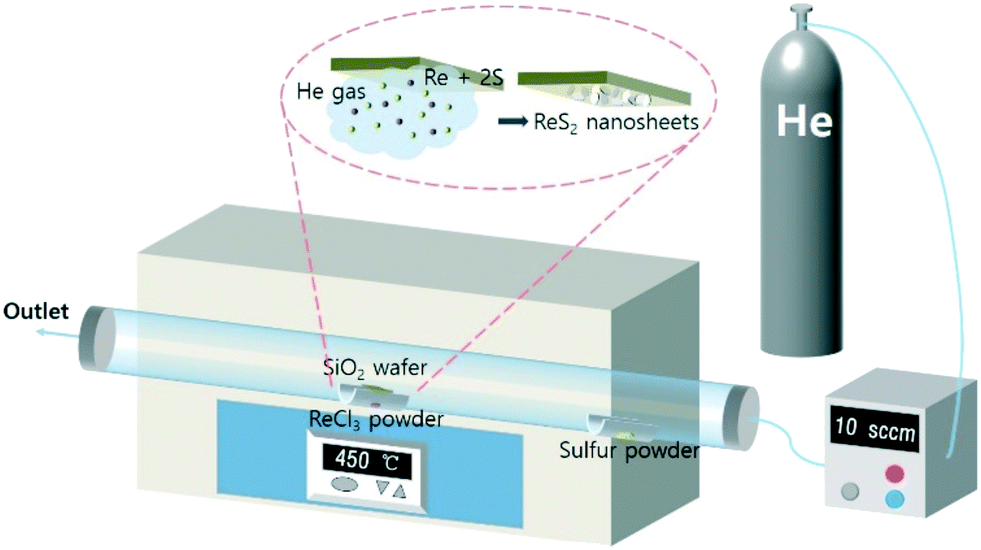 | ||
| Fig. 1 Schematic diagram for the growth process of the ReS2 nanosheets. | ||
Fig. 2 presents typical SEM and atomic force microscopy (AFM) images of the as-grown ReS2 nanosheets at 450 °C. It is immediately apparent that a high density of the ReS2 nanosheets is well grown with mostly vertical orientations on the SiO2 substrate as shown in Fig. 2a and b. The high magnification SEM images in Fig. 2c and d clearly show that the size of the ReS2 nanosheets can be up to around 1 μm and their thickness is approximately less than 10 nm. Fig. 2c and d also indicate that the edges of the ReS2 nanosheets are connected with other out-of-plane nanosheets. In particular, it is reported that asymmetric crystal growth and out-of-plane growth as shown in Fig. 2 might be favorable due to the distorted 1T structure and weak interlayer coupling of ReS2. Additionally, the vertical orientation of the ReS2 nanosheets is partly attributed to the weak interaction between ReS2 and the SiO2 substrate due to the position of the SiO2/Si substrate with respect to the ReCl3 source as illustrated in Fig. 1. The representative AFM image in Fig. 2e shows that the height of a ReS2 nanosheet was measured to be 6.6 nm (along the line scan profile of the inset), which confirms the presence of approximately four or five layers of the ReS2 nanosheets.16 To reveal the influence of the growth temperature on the growth of the ReS2 nanosheets, we have explored the growth behaviors at different growth temperatures as shown in Fig. S1.† As shown in Fig. S1(a),† although the growth of the ReS2 nanosheets already starts at 350 °C, the size of the ReS2 nanosheets is too small and their morphology is not well-defined. With the increase in growth temperature from 400 °C to 550 °C, the size of the ReS2 nanosheets gradually increases due to the faster growth rate at higher temperature.
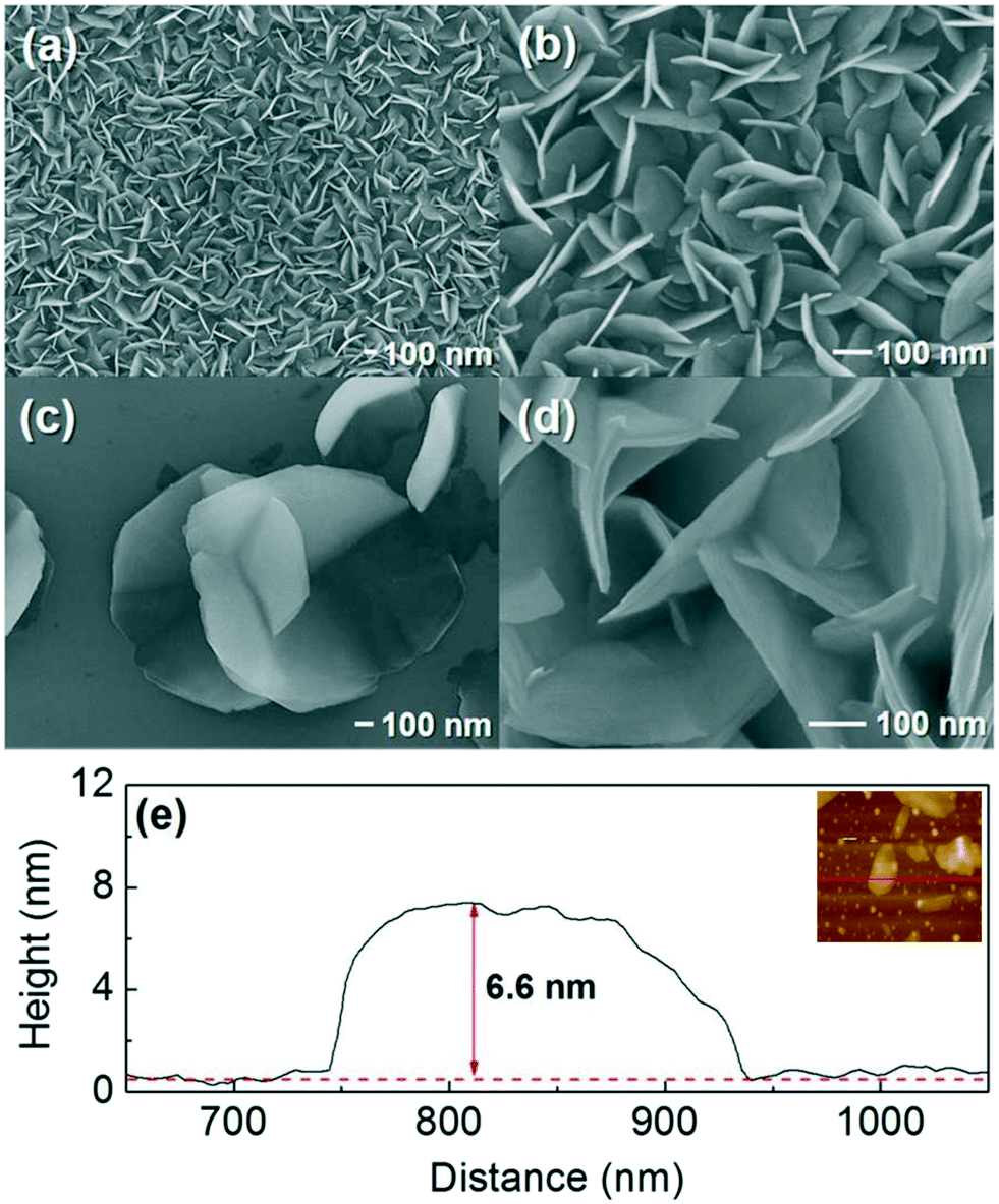 | ||
| Fig. 2 (a)–(d) Low and high magnification SEM images of the ReS2 nanosheets grown at 450 °C under a He carrier gas flow of 10 sccm for 20 minutes. (e) Height profile of a ReS2 nanosheet on the SiO2/Si substrate along the line of the inset. | ||
As seen in Fig. S1(e),† particularly, the sample grown at 550 °C presents a much higher density than that at 450 °C and it appears in the form of a continuous thin film covering the entire substrate. In contrast, the growth at 600 °C indicates the formation of very thick flake-like ReS2 nanostructures, which represents a quite distinct morphology.
Fig. 3a shows the XRD pattern of the ReS2 nanosheets grown at 450 °C, indicating that there are only four prominent peaks at 14.80, 29.60, 44.88, and 61.82°, respectively. The most intense peak at 14.80° is attributed to the (001) crystallographic plane of a triclinic ReS2 crystal structure and the lattice constant of the c axis is estimated to be 0.6282 nm, which is close to the reference value of 0.6375 nm.17–19 All other peaks match well with the (002), (003), and (004) crystal planes belonging to the triclinic ReS2 crystal structure (ICDD, reference number: 00-052-0818).17–19 The observation of only (00l) reflections with all other (hkl) reflections being absent implies that the ReS2 crystal structure is highly oriented along the c axis direction. In addition, it is worth mentioning that the sharp characteristic indexed peaks confirm the degree of the crystallinity of the two-dimensional layered structures. The Raman spectrum of the as-grown ReS2 nanosheets was collected at 632.8 nm laser excitation as illustrated in Fig. 3b. The series of Raman modes shown in Fig. 3b are reasonably consistent with previously reported values for a few layered ReS2 nanostructures.18–20 It is readily identified that the most intense peak at 150 cm−1 is a typical first order in-plane E2g vibrational mode, while the peak at 210 cm−1 is a characteristic Raman mode for out-of-plane (A1g like) vibration, respectively.18 It is well described that the additional Raman modes shown in the region of 100–400 cm−1 are attributed to symmetry splitting in the distorted 1T structure of ReS2. Some satellite Raman peaks in the region of 300–400 cm−1 also originated from the second order Raman modes.19
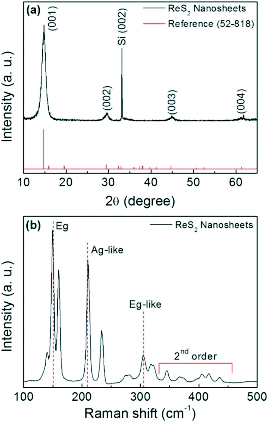 | ||
| Fig. 3 Structure and composition characterization of the ReS2 nanosheets grown at 450 °C under a He carrier gas flow of 10 sccm for 20 minutes. (a) X-ray diffraction spectrum with the triclinic ReS2 crystal structure as the reference XRD structure (ICDD, reference number: 00-052-0818); (b) Raman spectrum measured at 632.8 nm laser excitation. Note that the diffraction peak at 33.2° is attributed to the (002) plane of Si on a SiO2/(001) oriented Si substrate due to multiple diffractions which are essentially consecutive diffractions by different planes.21 | ||
Fig. 4 and S2† show the XPS results revealing the surface composition and the chemical states of the elements in the ReS2 nanosheets. Fig. S2† presents the survey spectrum of the as-grown ReS2 nanosheets, displaying five elements such as Re, S, Si, C, and O. It is apparent that the Si and O elements came from the SiO2 substrate while the peak of carbon (C) originated from an environmental contaminant. The XPS spectrum for Re 4f in Fig. 4a shows two predominant peaks at binding energies of 42.6 eV and 45.1 eV, which are readily assigned to the characteristic profile of the Re4+ 4f final states consistent with literature values.19,20 The characteristic S 2p3/2 binding energy of the divalent ion (S2−) oxidation state is located at 163.1 eV as shown Fig. 4b. Although the region of the core-level S 2p peaks is relatively broad in our XPS, the peak at 164.2 eV which can be assigned to the S 2p1/2 state is also a characteristic binding energy of the divalent ion (S2−) in Fig. 4b.19,20 These features are thus consistent with the XPS spectra of the exfoliated bulk ReS2 crystal. The atomic ratio of Re/S obtained by XPS is carefully estimated at 1![[thin space (1/6-em)]](https://www.rsc.org/images/entities/char_2009.gif) :1.98, demonstrating that the grown ReS2 nanosheets are very much stoichiometric.
:1.98, demonstrating that the grown ReS2 nanosheets are very much stoichiometric.
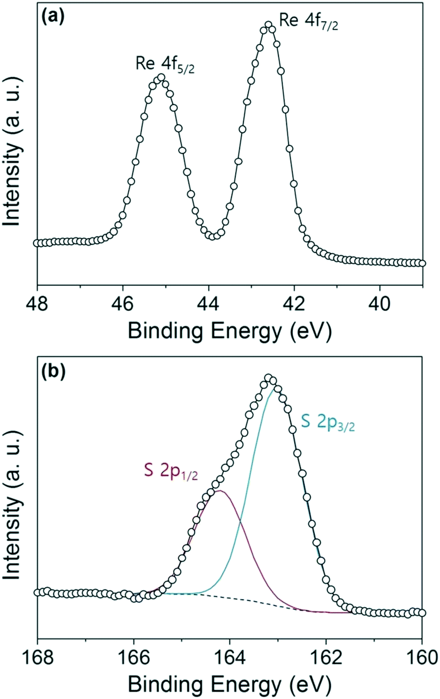 | ||
| Fig. 4 X-ray photoelectron spectroscopy (XPS) for the ReS2 nanosheets grown at 450 °C under a He carrier gas flow of 10 sccm for 20 minutes. (a) and (b) The high resolution spectra for Re 4f and S 2p. | ||
The detailed crystallographic structure of the grown ReS2 nanosheets was carefully characterized by HR-(S)TEM and fast Fourier transform (FFT) imaging by transferring the ReS2 nanosheets onto a TEM grid, as shown in Fig. 5. The Z-contrast high-angle annular dark field scanning transmission electron microscopy (HAADF-STEM) image obviously indicates the formation of different numbers of layered ReS2 nanosheets, represented by the relative difference in brightness with distinct edges as shown in Fig. 5a and b. The top view of the filtered Z-contrast HAADF-STEM image of ReS2 is shown in Fig. 5d. To confirm the existence of specific crystalline planes corresponding to ReS2, a Fourier filtering process was done as shown in Fig. 5d. Four Re atoms (represented by blue spheres in the schematics in Fig. 5d) are arranged in a diamond-like shape, and the diamonds form atomic chains in the b[010] direction with a spacing of 0.39 nm between the chains. Fig. S3† presents the top view of the filtered HRTEM image of ReS2 and the corresponding FFT image along the [241] zone axis. These images also confirm the existence of specific crystalline planes corresponding to the ReS2 crystal structures, indicating the highly single-crystalline nature of the nanosheets, consistent with XRD measurement. Furthermore, EDX elemental mapping analysis of the material using the HAADF-STEM image shown in Fig. S4† indicates the presence of Re and S atoms. These atoms are homogeneously distributed within the entire nanosheet structure.
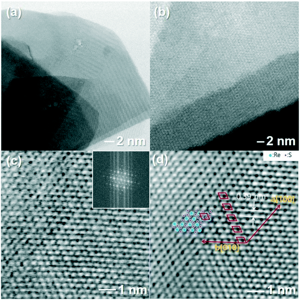 | ||
| Fig. 5 (a)–(c) Z-contrast high-angle annular dark field (HAADF) STEM images of the ReS2 nanosheets grown at 450 °C under a He carrier gas flow of 10 sccm for 20 minutes. The inset of (c) shows the diffraction pattern of the nanosheets. (d) Fourier filtered image of (c) with schematics of the triclinic ReS2 crystal structure. | ||
EDX measurement also confirmed that the ReS2 nanosheets consist of only Re and S atoms. In addition, TEM-EDS measurement in Fig. S5† indicates that the atomic ratio of Re/S is carefully estimated at 1:2.22, demonstrating that the as-grown ReS2 nanosheets are reasonably close to being stoichiometric, but it is slightly higher than that of the XPS result.
As illustrated in Fig. 1, the growth of the ReS2 nanosheets in this study could be achieved by the direct chemical reaction between Re atoms and S atoms on a SiO2 substrate under the stream of the carrier gas (He) at 450 °C. It is suggested that at the growth temperature (450 °C), ReCl3 in this study can decompose into Re and Cl2 and then the Re atoms can directly react with the S atoms on the SiO2 substrate to form tiny ReS2 nuclei. The continuous feeding of Re atoms and S atoms into the nucleation sites near the ReS2 nuclei can then lead to the two-dimensional layered structure of ReS2 as the favorable form. In fact, the supply of Re atoms originating from the gas phase of ReCl3 plays a critical role in efficiently obtaining the ReS2 nanosheets with high crystallinity and high density. However, previous studies showed that when ReO3 was used as the Re source in the CVD process, the resulting ReS2 nanosheets obtained at approximately 450 °C are very amorphous with a significantly low density owing to the formation of other rhenium containing metal oxides such as Re2O7 and ReO2.19,20 Thus, it was suggested that appropriate temperature control and sulfur introduction time are considerably essential for the formation of high quality ReS2 nanosheets.19,20 In contrast, the Re atoms in our growth mode are obtained from the direct decomposition of ReCl3 under the flow of the carrier gas (He), thus the formation of rhenium oxides is not favourable. Hence, the concentration of Re atoms is appropriate for the continuous growth of many nucleation sites of ReS2 on the SiO2 substrate.
Accordingly, we have successfully prepared highly crystalline ReS2 nanosheets with a few layers by a simple chemical reaction using ReCl3 as the Re precursor and sulfur at relatively low temperature compared with other reported growth processes. The synthetic approach for the ReS2 nanosheets exhibits several favorable features: it is simple, cost-effective, and versatile for the development of new functional platforms toward highly single-crystalline 2D layered materials.
Acknowledgements
This work was financially supported by the National Research Foundation of Korea (NRF), funded by the Korean Government (2016R1D1A1B03934962 for MHK).References
- Z. Lin, A. McCreary, N. Briggs, S. Subramanian, K. Zhang, Y. Sun, X. Li, N. J. Borys, H. Yuan, S. K. Fullerton-Shirey, A. Chernikov, H. Zhao, S. McDonnell, A. M. Lindenberg, K. Xiao, B. J. LeRoy, M. Drndic, J. C. M. Hwang, J. Park, M. Chhowalla, R. E. Schaak, A. Javey, M. C. Hersam, J. Robinson and M. Terrones, 2D Mater., 2016, 3, 042001 CrossRef
.
- B. Liu, L. Chen, G. Liu, A. N. Abbas, M. Fathi and C. Zhou, ACS Nano, 2014, 8, 5304–5314 CrossRef CAS PubMed
- Y.-C. Lin, H.-P. Komsa, C.-H. Yeh, T. Bjorkman, Z.-Y. Liang, C.-H. Ho, Y.-S. Huang, P.-W. Chiu, A. V. Krasheninnikov and K. Suenaga, ACS Nano, 2015, 9, 11249–11257 CrossRef CAS PubMed
- Y.-H. Lee, X.-Q. Zhang, W. Zhang, M.-T. Chang, C.-T. Lin, K.-D. Chang, Y.-C. Yu, J. T.-W. Wang, C.-S. Chang, L.-J. Li and T.-W. Lin, Adv. Mater., 2014, 24, 2320–2325 CrossRef PubMed
- K. Keyshar, Y. Gong, G. Ye, G. Brunetto, W. Zhou, D. P. Cole, K. Hackenberg, Y. He, L. Machado, M. Kabbani, A. H. C. Hart, B. Li, D. S. Galvao, A. George, R. Vajtai, C. S. Tiwary and P. M. Ajayan, Adv. Mater., 2015, 27, 4640–4648 CrossRef CAS PubMed
- F. Liu, S. Zheng, X. He, A. Chaturvedi, J. He, W. L. Chow, T. R. Mion, X. Wang, J. Zhou, Q. Fu, H. J. Fan, B. K. Tay, R.-H. He, C. Kloc, P. M. Ajayan and Z. Liu, Adv. Mater., 2016, 26, 1169–1177 CAS
- C. Sepulveda, R. Garcia, N. Escalona, D. Laurenti, L. Massin and M. Vrinat, Catal. Lett., 2011, 141, 987–995 CrossRef CAS
- C. Sepulveda, N. Escalona, R. Garcia, D. Laurenti and M. Vrinat, Catal. Today, 2012, 195, 101–105 CrossRef CAS
- D. Laurenti, K. T. N. Thi, N. Escalona, L. Massin, M. Vrinat and F. J. G. Llambias, Catal. Today, 2008, 130, 50–55 CrossRef CAS
- N. Al-Dulami, E. A. Lewis, D. J. Lewis, S. K. Howell, S. J. Haigh and P. O'Brien, Chem. Commun., 2016, 52, 7878–7881 RSC
- L. Wang, Z. Sofer, J. Luxa, D. Sedmidubsky, A. Ambrosi and M. Pumera, Electron. Commun., 2016, 63, 39–43 CrossRef
- T. C. Ho, Q. Shen, J. M. McConnachie and C. E. Kliewer, J. Catal., 2010, 276, 114–122 CrossRef CAS
- X. Wang, H. Feng, Y. Wu and L. Jiao, J. Am. Chem. Soc., 2013, 135, 5304–5307 CrossRef CAS PubMed
- L. Hart, S. Dale, S. Hoye, J. L. Webb and D. Wolverson, Nano Lett., 2016, 16, 1381–1386 CrossRef CAS PubMed
- J. Gao, L. Li, J. Tan, H. Sun, B. Li, J. C. Idrobo, C. V. Singh, T.-M. Lu and N. Koratkar, Nano Lett., 2016, 16, 3780–3787 CrossRef CAS PubMed
- D. A. Chenet, O. B. Aslan, P. Y. Huang, C. Fan, A. M. van der Zande, T. F. Heinz and J. C. Hone, Nano Lett., 2015, 15, 5667–5672 CrossRef CAS PubMed
- J. C. Shaw, H. Zhou, Y. Chen, N. O. Weiss, Y. Liu, Y. Huang and X. Duan, Nano Res., 2014, 7, 511–517 CrossRef CAS
- Q. H. Wang, K. Kalantar-Zadeh, A. Kis, J. N. Coleman and M. S. Strano, Nat. Nanotechnol., 2012, 7, 699–712 CrossRef CAS PubMed
- Y. Zhan, Z. Liu, S. Najmaei, P. M. Ajayan and J. Lou, Small, 2012, 8, 966–971 CrossRef CAS PubMed
- X. He, F. Liu, P. Hu, W. Fu, X. Wang, Q. Zeng, W. Zhao and Z. Liu, Small, 2015, 11, 5423–5429 CrossRef CAS PubMed
- B. H. Hwang, J. Phys. D: Appl. Phys., 2001, 34, 2469–2474 CrossRef CAS
Footnotes |
| † Electronic supplementary information (ESI) available: Additional XPS analysis, HRTEM images, and EDX elemental mapping analysis of the material using the HAADF-STEM image of the highly single-crystalline ReS2 nanosheets with a few layers. See DOI: 10.1039/c7ce00926g |
| ‡ These authors contributed equally to this work. |
| This journal is © The Royal Society of Chemistry 2017 |