
Constructing hierarchical hollow CuS microspheres via a galvanic replacement reaction and their use as wide-band microwave absorbers†
Biao
Zhao
 *ab,
Xiaoqin
Guo
a,
Yuanyuan
Zhou
a,
Tingting
Su
c,
Chao
Ma
c and
Rui
Zhang
*a
*ab,
Xiaoqin
Guo
a,
Yuanyuan
Zhou
a,
Tingting
Su
c,
Chao
Ma
c and
Rui
Zhang
*a
aHenan Key Laboratory of Aeronautical Materials and Application Technology, School of Mechatronics Engineering, Zhengzhou University of Aeronautics, Zhengzhou, Henan 450046, China. E-mail: biao_zhao@zzia.edu.cn; zhangray@zzia.edu.cn; Fax: +86 371 60632600; Tel: +86 371 60632007
bDepartment of Mechanical and Industrial Engineering, University of Toronto, 5 King's College Road, Toronto, Ontario M5S 3G8, Canada
cSchool of Materials Science and Engineering, Zhengzhou University, Zhengzhou, Henan 450001, China
First published on 27th February 2017
Abstract
In this study, hollow three-dimensional CuS hierarchical microspheres were prepared via a facile galvanic replacement reaction. The hollow flower-like CuS microspheres were characterized by XRD, Raman, XPS, SEM and TEM techniques, which revealed that numerous nanoflakes were self-assembled to construct hollow flowers. Based on time-dependent experiments, a plausible formation mechanism (galvanic replacement reaction) was proposed. Paraffin-based composites, containing 50 wt% hollow CuS, exhibited outstanding microwave absorption capabilities, which were attributed to the suitable impedance match and dielectric loss. The minimal reflection loss was −17.5 dB and the effective bandwidth was 3.0 GHz with thin absorber thickness of 1.1 mm. In addition, we put forward a novel solution to evaluate the microwave absorption efficiency. The high efficiency microwave absorption properties originate from the electric/dielectric polarization and unique hollow flower-like structure. The hollow structures can adjust the dielectric properties to obtain good impedance matching. Moreover, the two-dimensional flakes and hollow flowers can induce more multiple reflection and scattering, which consumes more microwave energy. This study has led to a novel useful method for the design of hollow structures used as high efficiency microwave absorbers.
1. Introduction
Currently, the pollution from electromagnetic interference (EMI) has gained much more attention with the rapid development of communication devices and extensive use of electronic devices. Serious EM pollution not only disturbs the operation of electronic equipment but also influences human health and raises problems concerning the field of military applications. Therefore, it is urgent to find a highly effective shielding strategy to suppress or eliminate the ensuing problems caused by EMI.1–3 For practical applications, suitable microwave absorption materials should hold some important features including being lightweight and having low thickness, strong absorption capability and wide absorption bandwidth.4 Among all the candidates used for microwave attenuation, semiconductors, such as ZnO,5,6 SiC,7,8 MnO2,9,10 MoS2,11 TiO2 (ref. 12 and 13) and SnO2,14–16 have been extensively investigated. Semiconductor nanoparticles, due to the quantum size effect, can induce the splitting of the electron energy band,17 which is very close to the microwave energy, and the new band gap can result in microwave absorption. Thus, much more attention has been attracted to exploit semiconductor microwave absorbers.It is well known that an efficient absorber is expected to demonstrate good impedance matching and a strong attenuation capability. However, for practical application, the microwave performance of these semiconductor absorbers still needs to be improved because of their weak attenuation and unbalanced relationship between the complex permittivity and permeability (namely, impedance matching), giving rise to poor microwave absorption. In general, modifying the shape and morphology of the absorber is an effective method to tune the electromagnetic parameters and increase the microwave absorption properties. Hollow structured materials are promising microwave absorbers because they not only possess a lightweight characteristic but also have tunable complex permittivities to obtain a suitable impedance match using an appropriate hollow configuration.18–21 It is noteworthy that Che and co-workers initially investigated the microwave absorption properties of core@void@shell ellipsoidal Fe3O4@CuSiO3 nanorattles,19 the high temperature microwave absorption of yolk–shell Fe3O4@ZrO2 (ref. 20) and the magnetic coupling of CoNi@void@TiO2 microspheres.21 However, hollow structures are usually fabricated using a template process in the presence of entities such as silica beads, polymer beads, micelles or by seed-mediated methods.22–25 The template methods often require a complex process and consume much more energy and time. Recently, the galvanic replacement reaction, which is based on the different reduction potential between two materials, was verified to be an effective way to design hollow structures.26–29
Copper sulfide (CuS), as one of the most important semiconductor transition-metal chalcogenides, has been the focus of intense research due to its optical, electronic and other physical and chemical characteristics.30–32 Currently, CuS materials with various morphologies (symmetrical nanostructure, hexagonal nanoplatelets and cuboctahedron) have been successfully prepared and have been proven to display high efficiency microwave absorption properties.31,33,34 However, the microwave absorption properties of hollow hierarchical CuS have been scarcely reported. In this study, hollow flower-like CuS hierarchical microspheres were prepared via a facile galvanic replacement reaction. The hollow CuS microspheres exhibit competitive microwave absorption properties being lightweight, with a thin thickness and wide-band gap.
2. Experimental
All of the chemical reagents were commercial available and used without further purification. In this process, the hollow three-dimensional CuS hierarchical microspheres were prepared via a facile two-step method. First, Ni microspheres with a mean diameter of 1.0 μm were synthesized via a solution reduction step, which was similar to our previous reports.35–39 Subsequently, the hollow 3-D complex CuS hierarchical microspheres were prepared via a galvanic replacement reaction.26,27 The detailed procedures are given in the following paragraph.2.1. Preparation of hollow 3-D complex CuS hierarchical microspheres
Typically, Ni microspheres (0.05 g) were dispersed in ethylene glycol (60 mL). Then, 0.002 mol of CuSO4·5H2O, 0.001 mol of CTAB and 0.002 mol of sulfur powder (S) were added in order to the mixture with magnetic stirring. The resulting solution was then transferred into a Teflon-lined stainless-steel autoclave (80 mL capacity). Subsequently, the autoclave was sealed and maintained at 160 °C for 15 h. When the autoclave had naturally cooled to room temperature, the black products were collected and washed with absolute ethanol and distilled water several times and dried at 60 °C.2.2. Characterization
The crystalline structure and phases of the samples were identified by X-ray diffraction (XRD, Rigaku Ultima IV) using Cu Kα radiation (λ = 0.15418 nm). The morphologies and sizes of the different CuS microspheres were determined using field-emission scanning electron microscopy (FE-SEM, JEOL JSM-7001F, Japan), as well as with transmission electron microscopy (TEM, JEOL JEM-2100F, Japan). The elemental chemical states of the samples were recorded using X-ray photoelectron spectroscopy (XPS, XSAM 800, Kratos Co., U.K.) with Al Kα excitation radiation (1486.6 eV). The nitrogen sorption of the samples was measured using an Autosorb iQ obtained from Quantachrome Instruments. The apparent surface area was calculated using the BET method at 77 K. The pore size distribution plots were recorded from the desorption branch of the isotherms based on the Barrett–Joyner–Halenda (BJH) model. Laser Raman spectroscopy data were obtained using a LabRAM HR Evolution Confocal Laser MicroRaman spectrometer at room temperature.To investigate the microwave absorption properties of the as-obtained hollow microspheres, paraffin wax was selected as the matrix material, which was transparent to electromagnetic radiation. The synthesized hollow CuS hierarchical microspheres were dispersed into the molten paraffin matrix in various ratios. The paraffin-based mixture was pressed into a ring shape with an inner diameter of 3.0 mm and an outer diameter of 7.0 mm. The relative complex permeability (εr = ε′ − jε′′) and permeability (μr = μ′ − jμ′′) of the sample-wax composites were obtained using an Agilent N5244A vector network analyzer system.
3. Results and discussion
The phases and crystal structures of pure Ni microspheres, and the hollow complex 3-D CuS hierarchical microspheres were characterized using XRD, as presented in Fig. 1. For pure Ni microspheres, shown in Fig. 1a, it can be found that there are three evident diffraction peaks, which can be well assigned to the (111), (200) and (220) planes of Ni (JCPDS card No. 04-0850). There are no characteristic peaks corresponding to NiO or Ni(OH)2 detected, reflecting its high pure phase. In Fig. 1b, all of the diffraction peaks of the product can be well indexed to the pure hexagonal phase of CuS (JCPDS card No. 06-0464). No additional peaks for other phases were observed, thus indicating high purity of the CuS products. Moreover, it was also proven that the Ni microspheres were consumed in this procedure.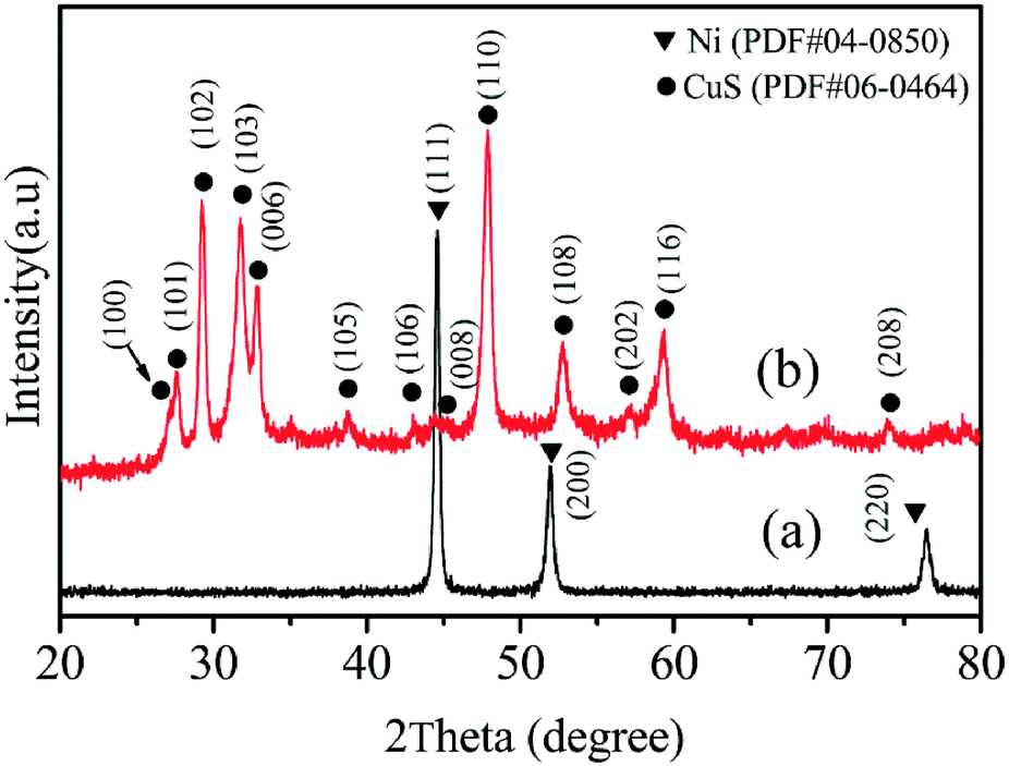 | ||
| Fig. 1 The XRD patterns of the (a) raw Ni microspheres and (b) hollow CuS hierarchical microspheres. | ||
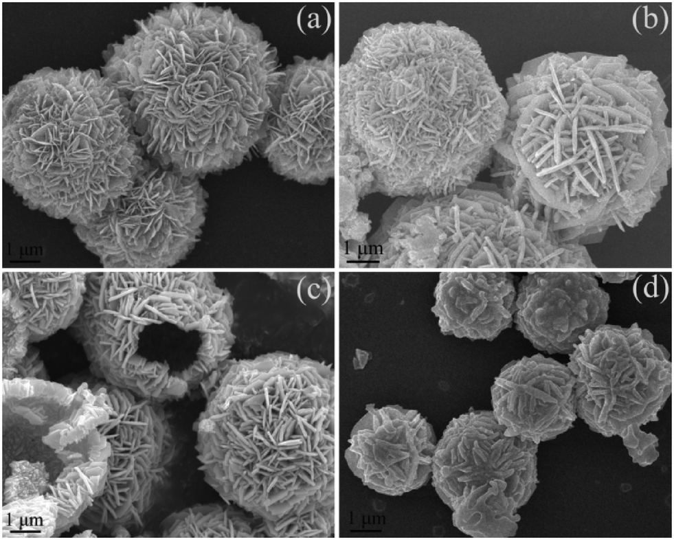
The inset in Fig. 2a is the SEM image of the raw Ni microspheres. It is noteworthy that the average diameter of the Ni microspheres with smooth surfaces was 1.0 μm. Scanning electron microscopy (SEM) images of the as-prepared copper sulfide (CuS) are shown in Fig. 2(a–d). From the overview images (Fig. 2a and b), the synthesized CuS products were microspheres with diameters of around 4 μm. Moreover, the synthesized products appear to possess superior dispersibility. Amazingly, the CuS microspheres show a hierarchical structure, which is consistent with the structure of peony flowers; they are both spherical, and both structures are composed of flakes. Upon further observation of some broken microspheres (Fig. 2a–d), it can be found that these hierarchical CuS peony flowers show hollow structures, which are conductive to the enhancement of microwave absorption. Fig. 2d presents the amplified image of one hollow microsphere, which indicates that the thickness of the nanoflakes was about 50 nm.
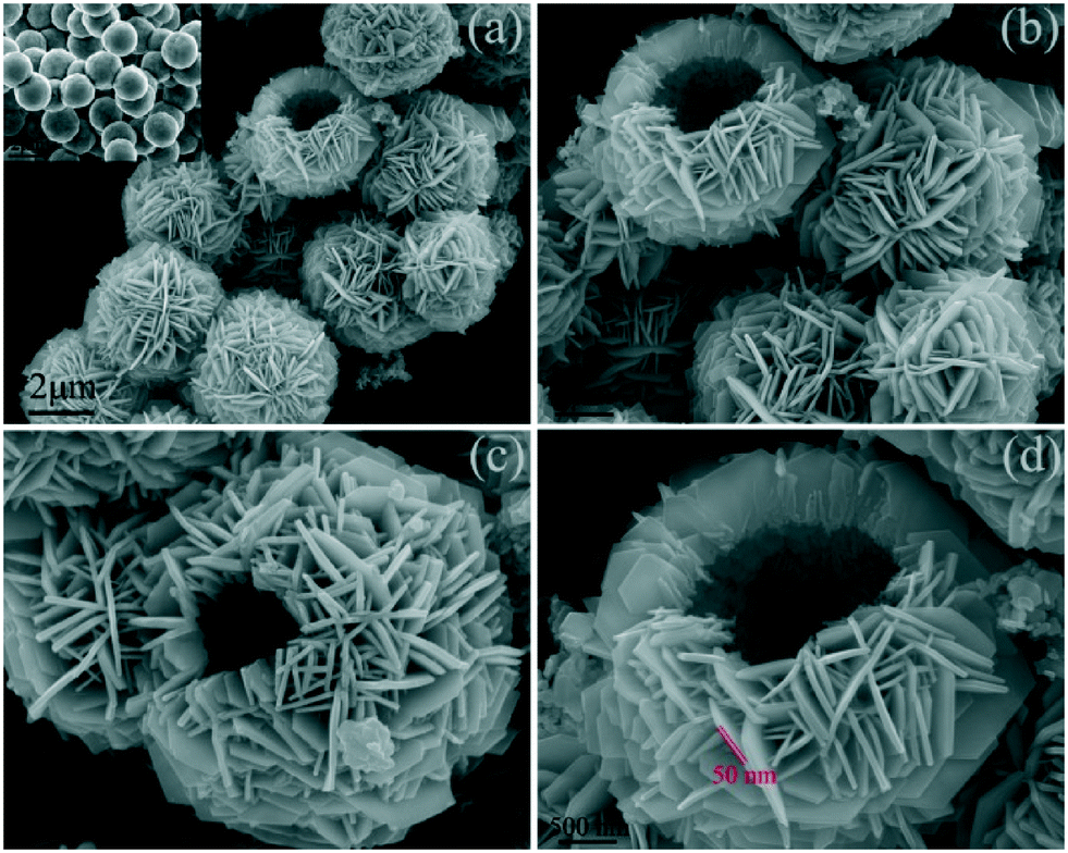 | ||
| Fig. 2 (a–d) Different magnification FESEM images of the hollow 3-D CuS hierarchical microspheres; the inset in Fig. 2a is the SEM image of the Ni microspheres. | ||
Fig. 3a shows the low-magnification TEM image of the synthesized hollow CuS peony flowers, which can clearly confirmed the hollow structures (different contrast between the light area in the center and black area at the fringe). Fig. 3b is HRTEM image, which was taken at the fringe. Through the HRTEM image, we found that the lattice spacing was 0.32 nm, which matches well with the distance between the (102) lattice planes,18,33 thus indicating the single-crystalline nature of the hollow hierarchical CuS peony flowers.
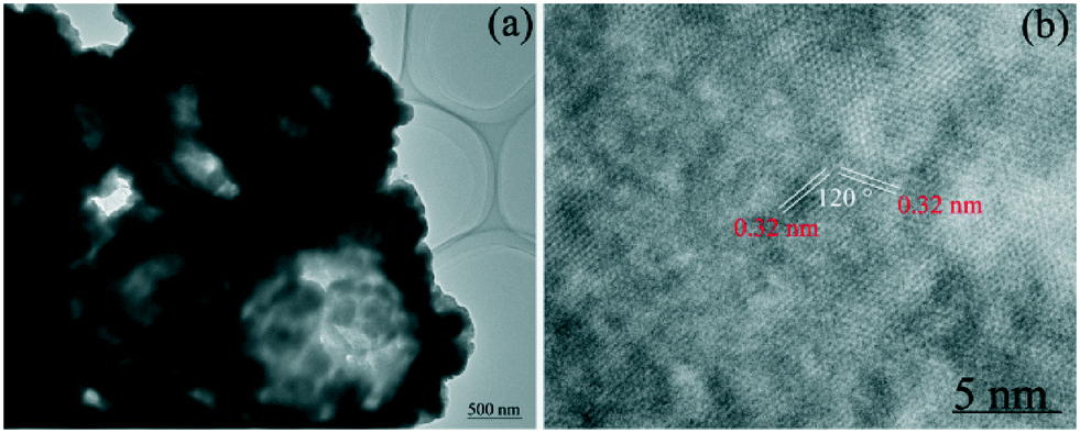 | ||
| Fig. 3 (a) The low-magnification TEM image and (b) HRTEM image of the synthesized hollow CuS peony flowers. | ||
The surface elemental chemical states of the hollow hierarchical CuS peony flowers were confirmed by X-ray photoelectron spectroscopy (XPS) measurements and the results are presented in Fig. 4a. Fig. 4a presents the high-resolution spectrum of Cu 2p; it is evident that the presence of two strong peaks at 931.7 and 951.8 eV can be assigned to Cu 2p3/2 and Cu 2p1/2, respectively. The binding energy between Cu 2p3/2 and Cu 2p1/2 was 20.1 eV, indicating the presence of Cu2+ ions in the hollow hierarchical CuS peony flowers.40 The XPS spectrum of S2p (inset in Fig. 4a) is characterized by a couple of peaks at 162.0 and 163.2 eV, which are consistent with the S2+ species.41 The abovementioned XPS analyses reveal the successful generation of hollow hierarchical CuS. The surface areas and pore size distributions of hollow hierarchical CuS peony flowers were investigated using their N2 adsorption–desorption isotherms. Fig. 4b shows that the CuS peony flowers have type II isotherms with H3 hysteresis loops on the basis of the Brunauer–Deming–Deming–Teller classification. Hysteresis loops between the adsorption and desorption suggest a porous structure. The shape of type H3 hysteresis loops is related to the formation of slit-like pores during the construction of the peony-like hollow microspheres. The surface area (SBET) and average pore size are 43.77 m2 g−1 and 15.33 nm, respectively. The BET surface area of these hollow complex CuS peony flowers was larger than those of hollow porous cobalt spheres42 (8.8 m2 g−1) and porous octahedral Ni (ref. 43) (3.123 m2 g−1). The higher surface area induces microwave multiple reflection and scattering, which is beneficial for the improvement of microwave absorption. Fig. S1† exhibits the Raman spectra of the hollow hierarchical CuS peony flowers. It can be found that a broad, strong peak was observed in the range of 400–600 cm−1. This peak was attributed to the presence of CuS, which is the same as previously reported.31,44
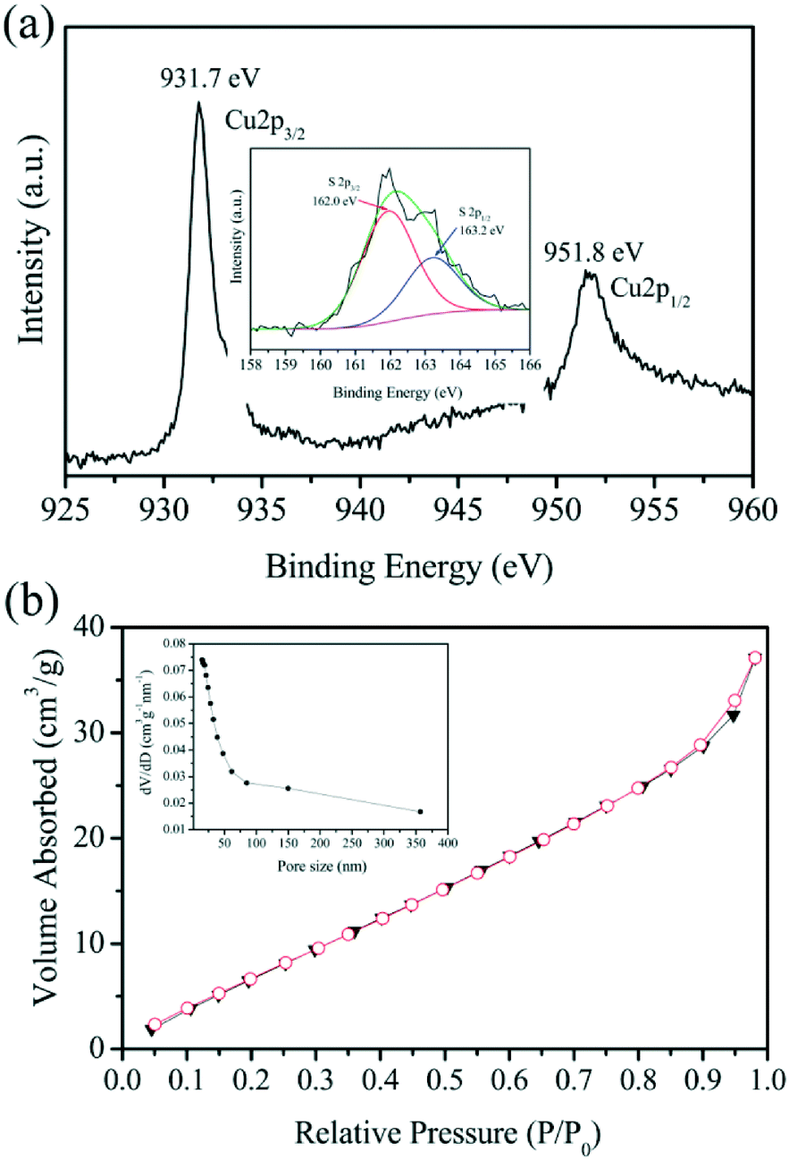 | ||
| Fig. 4 (a) The Cu 2p and S 2p XPS (inset in Fig. 4a) patterns of the hollow hierarchical CuS peony flowers. (b) The nitrogen adsorption/desorption isotherm and its corresponding pore size distribution (inset in Fig. 4b) curves obtained for the hollow hierarchical CuS peony flowers. | ||
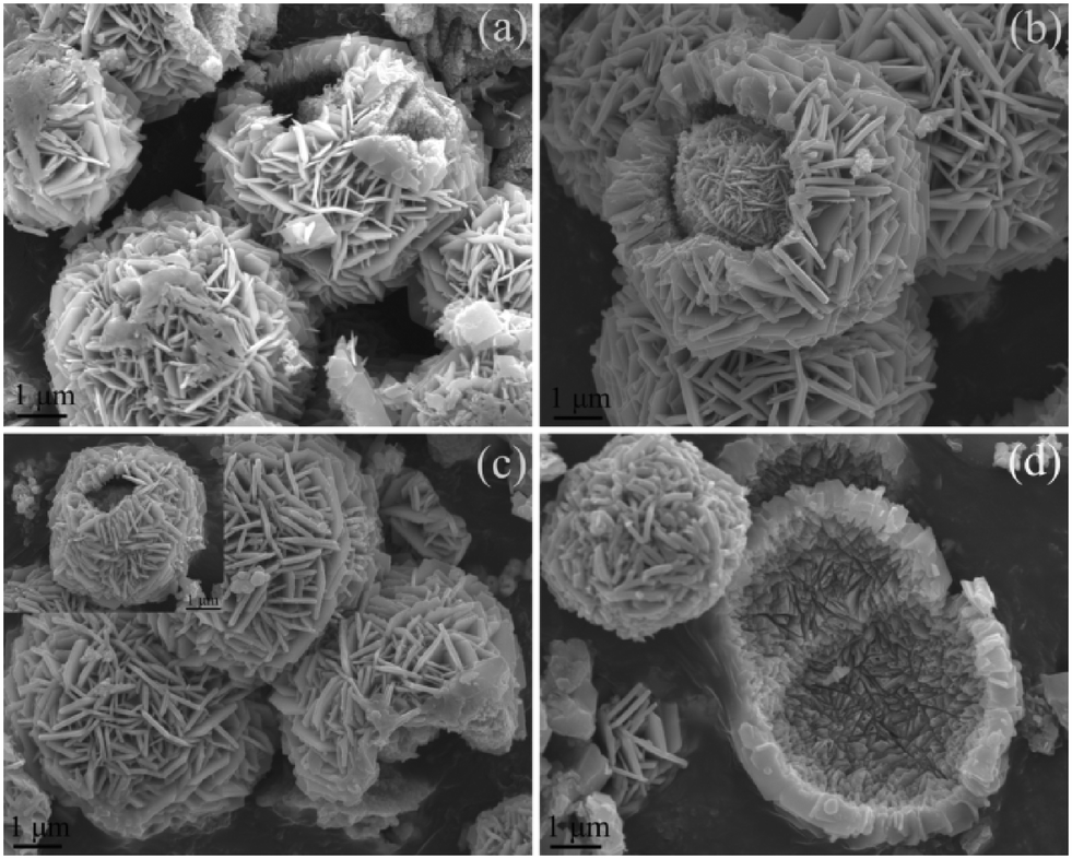
The influence of temperature on the morphologies and structures of the CuS product was investigated, and the results are shown in Fig. 5. The typical reaction temperature was chosen to be 140 °C to surpass the melting point of sulfur (about 120 °C). In our recipe, a complex hierarchical structure can be formed from 120 °C to 180 °C. If the reaction temperature drops below 120 °C, we cannot obtain CuS crystals. From Fig. 5, it can be found that the CuS samples exhibit similar structures (complex hierarchical flowers) in the range from 120 °C to 180 °C; however, differences are also apparent. First, flowers synthesized at 160 °C (Fig. 5c) show prominent hollow structures, which are not observed in the CuS samples made at 120 °C, 140 °C and 180 °C (Fig. 5a, b and d). Second, upon increasing the reaction temperature, the thickness of the nanoflakes becomes larger. Moreover, at relatively lower temperatures, the flowers are smoother than those made at higher temperature. From the abovementioned analysis, it can be concluded that the temperature influences the growth of the nanocrystals; a higher temperature leads to faster crystal growth, resulting in more defects on the surfaces.
 | ||
| Fig. 5 The SEM images of the CuS products obtained at different temperatures: (a) 120 °C, (b) 140 °C, (c) 160 °C and (d) 180 °C. | ||
To further reveal the formation mechanism of the hollow hierarchical CuS peony flowers, the final products were collected at reaction times of 3, 6, 10 and 15 h, and their phases and morphologies were analyzed by XRD and SEM, as shown in Fig. S2† and 6, respectively. Based on Fig. S2,† we can observe that all of the diffraction peaks of the samples prepared at various reaction times can match well with the CuS crystals, which verify that the Ni microspheres disappeared and the CuS nanocrystals were generated at the start of the reaction.
 | ||
| Fig. 6 FESEM image of the CuS products prepared at 160 °C under various reaction times: (a) 3 h, (b) 6 h, (c) 10 h and (d) 15 h. The inset of (c) is the enlarged FESEM image of the CuS product prepared at 10 h. | ||
Fig. 6 shows the representative FESEM images of the CuS products prepared at 160 °C after 3, 6, 10, and 15 h. As shown in Fig. 6a, the sample obtained at an early stage (3 h) comprised several dense flower-like microspheres (Fig. 6a). Furthermore, the hollow structure was also observed from the broken microspheres and the surfaces of hierarchical flowers were relatively rougher. The presence of some disordered nanoflakes could be found. When the reaction time was prolonged to 6 h, the smooth nanoflakes self-assembled to form perfect hierarchical peony flowers (Fig. 6b). Interestingly, a relatively small flower appeared inside the bigger flower. A unique core–void–shell structure was formed. The growth mechanism would be described in the following paragraph. As the reaction proceeded (10 h), the flower-like cores gradually disappeared due to the growth process45,46 and hollow hierarchical flower-like CuS appeared (Fig. 6c). When the reaction time was 15 h, the perfect complex flower-like hierarchical CuS hollow microspheres were obtained (Fig. 6d).
According to the abovementioned experimental results, the growth mechanism of the peony flower-like hierarchical CuS hollow microspheres could be a result of the galvanic replacement reaction,28 which is shown in Fig. 7. It is well known that the standard reduction potential of nickel [E0(Ni2+/Ni0) = −0.257 V] is lower than that of copper [E0(Cu2+/Cu0) = 0.342 V].47,48 Thus, the copper ions can be easily reduced to Cu(0) atom by the Ni metal via a galvanic replacement reaction (Ni + Cu2+ → Ni2+ + Cu), which is described by process (1). Subsequently, the fresh Cu(0) atoms will quickly react with sulfur (process (2)) to generate the CuS nanocrystals, and the fresh CuS nanocrystals were coated on the Ni surfaces to form yolk–shell structure. Based on Fig. 7, procedures (3) and (4) are the growth processes. Upon further consumption of Ni, the hollow CuS with double shells can be seen, which are attributed to growth process. Upon prolonging the reaction time, the inner CuS shell with high surface energy is dissolved and recrystallized to form the complex flower-like hierarchical CuS hollow microspheres. Thus, we can conclude that the formation of flower-like hierarchical CuS hollow microspheres is a result of the galvanic replacement reaction.
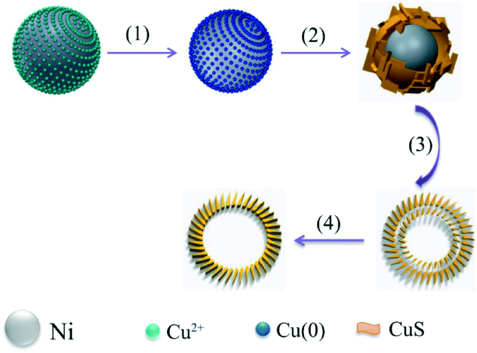 | ||
| Fig. 7 The proposed formation process of the flower-like hierarchical CuS hollow microspheres. | ||
The electromagnetic wave absorption properties of the dielectric materials are mostly determined by the complex relative permittivity (εr = ε′ − jε′′) and their microstructures. The real part (ε′) was correlated with the storage ability of the electric energy, and the imaginary part (ε′′) symbolizes the dissipation of the electric energy.49,50Fig. 8 shows the real parts (a) and imaginary parts (b) of the complex relative permittivity of the paraffin-composites containing different hollow hierarchical CuS loadings. Due to the presence of non-magnetic constituents in these paraffin-composites, the real part (μ′) and imaginary part (μ′′) of the complex relative permeability are approximately constant and close to 1 and 0, respectively, which is not shown here. From Fig. 8, it is very interesting to note that the real part (ε′) and imaginary part (ε′′) increase upon increasing the hollow hierarchical CuS loadings in the paraffin-composites. For the real part values (Fig. 8a), the ε′ values exhibit a decreasing tendency upon increasing the measured frequency, which results from the fact that the dielectric polarization cannot catch up with alternated electromagnetic field in the high GHz frequency region.6,51 For the imaginary part values (ε′′), according to free electron theory,52ε′′ ≈ 1/2πε0σf, where σ is the resistivity. Thus, it can be proposed that a high ε′′ value indicates high conductivity. In these CuS paraffin-based composites, we can deduce that a 60 wt% concentration of hollow CuS in the paraffin composites results in high conductivity of the composite, which is associated with the formation of conductive network with high CuS amounts. Generally, high ε′′ values and conductivity may be in favor of enhancing the microwave absorption properties. Notably, for the paraffin composites with 50 wt% concentrations of hollow CuS, an evident dielectric resonance was observed at around 15–17 GHz. The resonance was correlated with the dipole and electron polarization.7,11 Fig. S3† shows the dielectric loss tangents (tan![[thin space (1/6-em)]](https://www.rsc.org/images/entities/char_2009.gif) δε = ε′′/ε′) of the hierarchical hollow CuS paraffin composites with various amounts of hollow CuS. Generally, a higher tangent value suggests a higher loss and a better microwave attenuation capability.53 It was found that the values of the dielectric loss tangent increase with an increasing concentration of hollow CuS in the composites. Thus, we made the conclusion that the paraffin composite with a 50 wt% concentration of hierarchical hollow CuS may possess excellent microwave absorption abilities.
δε = ε′′/ε′) of the hierarchical hollow CuS paraffin composites with various amounts of hollow CuS. Generally, a higher tangent value suggests a higher loss and a better microwave attenuation capability.53 It was found that the values of the dielectric loss tangent increase with an increasing concentration of hollow CuS in the composites. Thus, we made the conclusion that the paraffin composite with a 50 wt% concentration of hierarchical hollow CuS may possess excellent microwave absorption abilities.
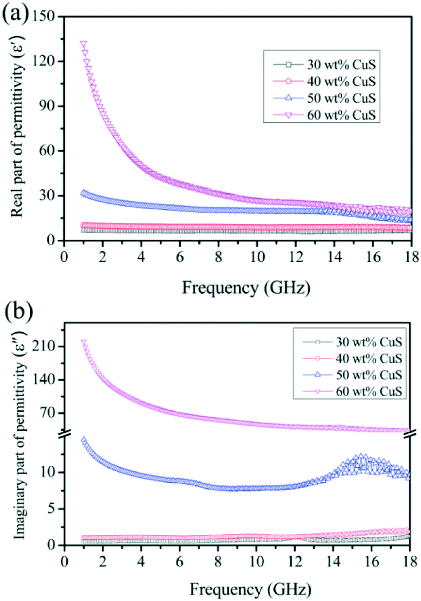 | ||
| Fig. 8 The frequency dependence of the real parts (a) and imaginary parts (b) of the complex relative permittivity of paraffin-composites containing different hollow hierarchical CuS loadings. | ||
The measurement of the microwave absorption properties is based on the transmission/reflection model proposed by Nicolson.54 When the electromagnetic wave is incident on the surface of a material, a weak reflection of the electromagnetic radiation means a strong attenuation of electromagnetic wave energy and a better absorption ability. A material's microwave absorption capability may be evaluated as the reflection loss (RL). A smaller RL suggests highly efficient absorption. The RL can be simulated using the following equations:55–57
| RL = 20log10|(Zin − Z0)/(Zin + Z0)| | (1) |
 | (2) |
 | (3) |
Fig. 9 depicts the simulated reflection loss (RL) curves obtained for the hierarchical hollow CuS paraffin composites with CuS loadings of 30–60 wt% at a thickness of 1.5 mm. It is interesting to note that the 50 wt% hollow CuS paraffin composite shows the best microwave absorption properties. The minimum RL of −17.8 dB was observed at 11.5 GHz, and RL values below −10 dB (90% microwave absorption) were obtained in the 10.3–12.9 GHz range with an absorber thickness of only 1.5 mm. However, for the 60 wt% hollow CuS paraffin composite, it presents a very weak microwave attenuation ability. It seems contradictory to the above high dielectric loss of the 60 wt% CuS paraffin composite in terms of the imaginary parts (ε′′). On the contrary, it is very reasonable to obtain these results. To obtain suitable microwave absorbers, one important factor – impedance match should be considered. A good impedance match13,58,59 can make the electromagnetic radiation enter into the absorber as much as possible, which requires the complex permittivity to be near to the complex permeability. In this study, a high amount of CuS (60 wt%) in the paraffin composite endows it with highest dielectric loss and conductivity, which is far away from the complex permeability. Moreover, the high conductivity will induce an eddy current effect and reflection rather than absorption.60 Thus, 60 wt% hollow CuS paraffin composites show poor microwave absorption properties.
 | ||
| Fig. 9 The reflection losses of the hollow CuS paraffin composites with CuS loadings of 30–60 wt% at a thickness of 1.5 mm. | ||
From eqn ((1)–(3)), it can be found that the electromagnetic radiation absorption properties were also closely associated with the absorber thickness. To reveal the influence of thickness on the microwave absorption properties, the reflection loss and 3D image map (inset in Fig. 10a) of the 50 wt% hollow CuS paraffin composite with various absorber thicknesses are shown in Fig. 10a. It is notable that the optimal reflection loss moves towards a lower frequency upon increasing the thickness. The best absorption of the CuS paraffin composite corresponds to a λ/4 thickness, conforming to the quarter-wavelength matching model.19,61 The effective bandwidth of the RL values below −10 dB (90% microwave dissipation) can be tuned between 7.6 and 18.0 GHz with a thin absorber thickness of 1.1–2.0 mm. To date, it is difficult to evaluate the microwave absorption performance of absorbing materials because we need to consider plentiful factors, for example, the minimal RL peak, the bandwidth and the absorber thickness. Fig. 10(b–d) presents the reflection loss of the 50 wt% hollow CuS paraffin composites with various thicknesses of 1.1 mm, 1.2 mm and 1.3 mm. For the absorber thickness of 1.1 mm (Fig. 10b), the optimal absorption was −17.5 dB and the effective bandwidth was 3.0 GHz. Interestingly, with an increasing absorber thickness (Fig. 10c and d), the effective bandwidth exhibits an increasing tendency. For the absorber layer of 1.2 mm, the minimal reflection loss was −16.0 dB and the effective bandwidth was 4.2 GHz. Hence, it is difficult to judge the thickness that is suitable to obtain the best microwave absorption properties. Thus, herein, we put forward a new method to judge the microwave absorption efficiency. First, we made a definition of ΔS, which is equal to the area of shade when the RL is below −10 dB; it can be expressed as ΔS = ∫RLdf|RL≤−10dB.20 When the absorber thickness was 1.1 mm, 1.2 mm and 1.3 mm, the corresponding ΔS values were 12.53, 13.49 and 10.58 dB GHz, respectively. Second, the electromagnetic absorption efficiency RE can be given as RE = ΔS/d. The RE values of the three absorber thicknesses are 11.39, 11.24, and 8.14 dB GHz mm−1. Thus, it can be inferred that when the absorber thickness was set as 1.2 mm, the best microwave absorption properties were achieved (RLmin = −17.5 dB, bandwidth of 3.0 GHz, ΔS = 12.53 dB GHz and RE = 11.39 dB GHz mm−1).
 | ||
| Fig. 10 (a) The microwave absorption properties of the 50 wt% hollow CuS paraffin composites with a sample thickness from 1.1 to 2.0 mm and a frequency range of 1–18 GHz; the inset in Fig. 9a is the three-dimensional representation of the RL values obtained for the hollow CuS paraffin-based composite. The reflection loss of the 50 wt% hollow CuS paraffin composites with a thickness of: (b) 1.1, (c) 1.2 and (d) 1.3 mm. | ||
For dielectric materials, the dielectric loss mainly originates from electron polarization, ion polarization, and electric dipolar polarization. The electron polarization and the ion polarization can be excluded due to being weak in the microwave range and strongly occurring at a higher frequency than the infrared region.62,63 Thus, it can be deduced that the dielectric loss of hollow CuS paraffin-composites comes from the electric dipolar polarization. In the polarization processes, most of the electromagnetic energy is irreversibly transformed to Joule thermal energy. This process can be described by the Debye dipolar polarization as follows:64,65
 | (4) |
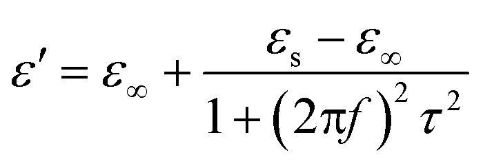 | (5) |
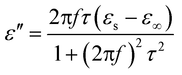 | (6) |
Based on eqn ((5) and (6)), it can deduce that ε′ is a function of ε′′ and f, namely, ε′ = ε′′/2πfτ + ε∞. Thus, if the dielectric loss only stems from the electric dipolar polarization, the plot of ε′ vs. B0 (B0 = ε′′/f) would be linear. It is expected that the hollow CuS paraffin-composite presents an approximate linear variation (Fig. 11), indicating that the electric dipolar polarization was dominant in this system. Moreover, the pattern of B0versus ε′ for the hollow CuS paraffin-composite sample can be fitted with three different slopes (k = 1/2πτ). Thus, we can obtain τ1 = 0.00908 × 10⁻⁹ s, τ2 = 0.0724 × 10⁻⁹ s, and τ3 = 0.2476 × 10⁻⁹ s. Based on eqn (5) and (6), we can infer that the frequencies of the Debye polarization (fr = 1/2πτ) are 17.533 GHz, 2.196 GHz, and 0.643 GHz, which is nearly consistent with the abovementioned ε′′ values shown in Fig. 7b.
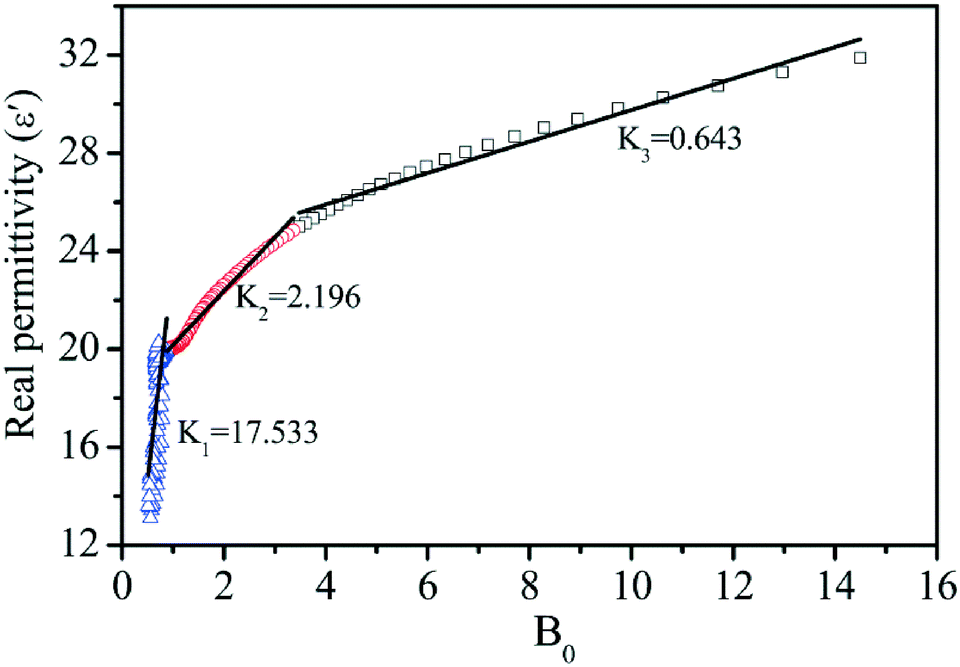 | ||
| Fig. 11 The plots of ε′ vs. B0 (B0 = ε′′/f) obtained for the 50 wt% hollow CuS paraffin-composite. | ||
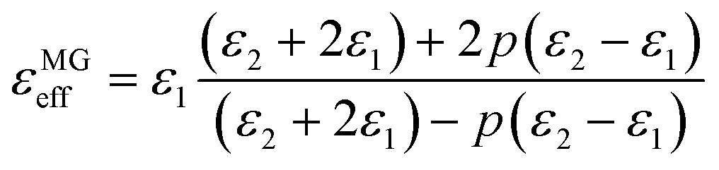
Apart from the contribution of electric dipolar polarization, the unique hollow hierarchical flower-like structures are also beneficial for the improvement of microwave absorption. On one hand, the two-dimensional CuS nanoflakes, which are self-assembled to form three-dimensional flowers, are proposed to be the consumed center. When microwaves strike the surface of the CuS nanoflakes, the waves penetrate through the CuS lattice structure where their interaction with the CuS induces currents that contribute to an ohmic loss, resulting in a drop in the energy of the microwaves.66 Moreover, when the microwaves encounter the nanoflakes, they are mainly reflected and scattered. On the other hand, the other portion of microwaves, which enters into the hollow structures, is reflected and scattered at the confined void. This multiple reflection combines with the adequate level of microwave absorption capability inside the composite matrix resulting in the further attenuation of the microwaves and thereby enhances the microwave absorption ability. Furthermore, based on the Maxwell Garnett (MG) theory:2,14
 | (7) |
4. Conclusion
In summary, the flower-like hierarchical CuS hollow microspheres were successfully prepared via a galvanic replacement reaction. The effect of the reaction recipes (reaction time and temperature) on the morphology and structure of the final CuS products were analyzed in detail, and the formation mechanism was also proposed based on the serial time-dependent experiments. The microwave absorption properties of the hollow CuS flowers paraffin composites with various CuS amounts were analyzed, and it was found that the 50 wt% hollow CuS paraffin composite exhibited outstanding microwave absorption capabilities, which were attributed to an appropriate impedance match and dielectric loss. Moreover, the unique hollow three-dimensional hierarchical structures assembled by the nanoflakes can induce multiple reflection and scattering, which is favorable to improve the microwave absorption properties. Thus, this study paves an effective avenue to design hollow structures as competitive microwave absorbers whilst being lightweight with a wide band gap and thin thickness.Acknowledgements
The authors appreciate the financial support from the National Natural Science Foundation of China (Grant No. 51672254).Notes and references
- D. Ding, Y. Wang, X. Li, R. Qiang, P. Xu, W. Chu, X. Han and Y. Du, Carbon, 2017, 111, 722–732 CrossRef CAS
.
- X. Li, B. Zhang, C. Ju, X. Han, Y. Du and P. Xu, J. Phys. Chem. C, 2011, 115, 12350–12357 CAS
- X. Xie, Y. Pang, H. Kikuchi and T. Liu, Phys. Chem. Chem. Phys., 2016, 18, 30507–30514 RSC
- P. Liu, Z. Yao, J. Zhou, Z. Yang and L. B. Kong, J. Mater. Chem. C, 2016, 4, 9738–9749 RSC
- Q. Hu, G. Tong, W. Wu, F. Liu, H. Qian and D. Hong, CrystEngComm, 2013, 15, 1314–1323 RSC
- G.-S. Wang, Y.-Y. Wu, X.-J. Zhang, Y. Li, L. Guo and M.-S. Cao, J. Mater. Chem. A, 2014, 2, 8644–8651 CAS
- H.-J. Yang, W.-Q. Cao, D.-Q. Zhang, T.-J. Su, H.-L. Shi, W.-Z. Wang, J. Yuan and M.-S. Cao, ACS Appl. Mater. Interfaces, 2015, 7, 7073–7077 CAS
- H.-L. Zhu, Y.-J. Bai, R. Liu, N. Lun, Y.-X. Qi, F.-D. Han and J.-Q. Bi, J. Mater. Chem., 2011, 21, 13581–13587 RSC
- M. Zhou, X. Zhang, J. Wei, S. Zhao, L. Wang and B. Feng, J. Phys. Chem. C, 2010, 115, 1398–1402 Search PubMed
- Y. Wang, H. Guan, S. Du and Y. Wang, RSC Adv., 2015, 5, 88979–88988 RSC
- Y. Wang, D. Chen, X. Yin, P. Xu, F. Wu and M. He, ACS Appl. Mater. Interfaces, 2015, 7, 26226–26234 CAS
- T. Xia, C. Zhang, N. A. Oyler and X. Chen, Adv. Mater., 2013, 25, 6905–6910 CrossRef CAS PubMed
- X. Zhang, G. Ji, W. Liu, X. Zhang, Q. Gao, Y. Li and Y. Du, J. Mater. Chem. C, 2016, 4, 1860–1870 RSC
- B. Zhao, B. Fan, Y. Xu, G. Shao, X. Wang, W. Zhao and R. Zhang, ACS Appl. Mater. Interfaces, 2015, 7, 26217–26225 CAS
- B. Zhao, X. Guo, W. Zhao, J. Deng, G. Shao, B. Fan, Z. Bai and R. Zhang, ACS Appl. Mater. Interfaces, 2016, 8, 28917–28925 CAS
- B. Zhao, B. Fan, G. Shao, W. Zhao and R. Zhang, ACS Appl. Mater. Interfaces, 2015, 7, 18815–18823 CAS
- D. Yan, S. Cheng, R. F. Zhuo, J. T. Chen, J. J. Feng, H. T. Feng, H. J. Li, Z. G. Wu, J. Wang and P. X. Yan, Nanotechnology, 2009, 20, 105706 CrossRef CAS PubMed
- B. Zhao, G. Shao, B. Fan, W. Zhao, Y. Xie and R. Zhang, J. Mater. Chem. A, 2015, 3, 10345–10352 CAS
- J. Xu, J. Liu, R. Che, C. Liang, M. Cao, Y. Li and Z. Liu, Nanoscale, 2014, 6, 5782–5790 RSC
- M. Yu, C. Liang, M. Liu, X. Liu, K. Yuan, H. Cao and R. Che, J. Mater. Chem. C, 2014, 2, 7275–7283 RSC
- Q. Liu, Q. Cao, H. Bi, C. Liang, K. Yuan, W. She, Y. Yang and R. Che, Adv. Mater., 2016, 28, 486–490 CrossRef CAS PubMed
- J. Liang, X.-Y. Yu, H. Zhou, H. B. Wu, S. Ding and X. W. Lou, Angew. Chem., Int. Ed., 2014, 53, 12803–12807 CrossRef CAS PubMed
- J. Yang and T. Sasaki, Chem. Mater., 2008, 20, 2049–2056 CrossRef CAS
- H. Liu, J. Qu, Y. Chen, J. Li, F. Ye, J. Y. Lee and J. Yang, J. Am. Chem. Soc., 2012, 134, 11602–11610 CrossRef CAS PubMed
- K. J. C. V. Bommel, J. H. Jung and S. Shinkai, Adv. Mater., 2001, 13, 1472–1476 CrossRef
- V. Bansal, H. Jani, J. Du Plessis, P. J. Coloe and S. K. Bhargava, Adv. Mater., 2008, 20, 717–723 CrossRef CAS
- Y. Liu and A. R. Hight Walker, ACS Nano, 2011, 5, 6843–6854 CrossRef CAS PubMed
- B. Goris, L. Polavarapu, S. Bals, G. Van Tendeloo and L. M. Liz-Marzán, Nano Lett., 2014, 14, 3220–3226 CrossRef CAS PubMed
- M. H. Oh, T. Yu, S.-H. Yu, B. Lim, K.-T. Ko, M.-G. Willinger, D.-H. Seo, B. H. Kim, M. G. Cho, J.-H. Park, K. Kang, Y.-E. Sung, N. Pinna and T. Hyeon, Science, 2013, 340, 964–968 CrossRef CAS PubMed
- Q. Tian, M. Tang, Y. Sun, R. Zou, Z. Chen, M. Zhu, S. Yang, J. Wang, J. Wang and J. Hu, Adv. Mater., 2011, 23, 3542–3547 CrossRef CAS PubMed
- S. He, G. S. Wang, C. Lu, X. Luo, B. Wen, L. Guo and M. S. Cao, ChemPlusChem, 2013, 78, 250–258 CrossRef CAS
- S.-W. Hsu, C. Ngo, W. Bryks and A. R. Tao, Chem. Mater., 2015, 27, 4957–4963 CrossRef CAS
- Y.-Z. Wei, G.-S. Wang, Y. Wu, Y.-H. Yue, J.-T. Wu, C. Lu and L. Guo, J. Mater. Chem. A, 2014, 2, 5516–5524 CAS
- S. He, G.-S. Wang, C. Lu, J. Liu, B. Wen, H. Liu, L. Guo and M.-S. Cao, J. Mater. Chem. A, 2013, 1, 4685–4692 CAS
- B. Zhao, G. Shao, B. Fan, W. Guo, Y. Chen and R. Zhang, Appl. Surf. Sci., 2015, 332, 112–120 CrossRef CAS
- B. Zhao, G. Shao, B. Fan, W. Zhao and R. Zhang, RSC Adv., 2014, 4, 57424–57429 RSC
- B. Zhao, G. Shao, B. Fan, W. Zhao and R. Zhang, Phys. Chem. Chem. Phys., 2015, 17, 2531–2539 RSC
- B. Zhao, G. Shao, B. Fan, W. Zhao, S. Zhang, K. Guan and R. Zhang, J. Mater. Chem. C, 2015, 3, 10862–10869 RSC
- B. Zhao, W. Zhao, G. Shao, B. Fan and R. Zhang, Dalton Trans., 2015, 44, 15984–15993 RSC
- Z. Guo, M. L. Seol, M. S. Kim, J. H. Ahn, Y. K. Choi, J. H. Liu and X. J. Huang, Nanoscale, 2012, 4, 7525–7531 RSC
- P. Liu, Y. Huang, J. Yan, Y. Yang and Y. Zhao, ACS Appl. Mater. Interfaces, 2016, 8, 5536–5546 CAS
- C. He, S. Qiu, X. Wang, J. Liu, L. Luan, W. Liu, M. Itoh and K.-I. Machida, J. Mater. Chem., 2012, 22, 22160–22166 RSC
- G. Tong, Q. Hu, W. Wu, W. Li, H. Qian and Y. Liang, J. Mater. Chem., 2012, 22, 17494–17504 RSC
- X.-J. Zhang, G.-S. Wang, Y.-Z. Wei, L. Guo and M.-S. Cao, J. Mater. Chem. A, 2013, 1, 12115–12122 CAS
- L. Cao, D. Chen and R. A. Caruso, Angew. Chem., Int. Ed., 2013, 52, 10986–10991 CrossRef CAS PubMed
- M. Cao, H. Lian and C. Hu, Nanoscale, 2010, 2, 2619–2623 RSC
- S. Zhang and H. C. Zeng, Chem. Mater., 2010, 22, 1282–1284 CrossRef CAS
- T. Yamauchi, Y. Tsukahara, T. Sakata, H. Mori, T. Yanagida, T. Kawai and Y. Wada, Nanoscale, 2010, 2, 515–523 RSC
- J. Deng, Q. Wang, Y. Zhou, B. Zhao and R. Zhang, RSC Adv., 2017, 7, 9294–9302 RSC
- H. Zhang, Y. Xu, J. Zhou, J. Jiao, Y. Chen, H. Wang, C. Liu, Z. Jiang and Z. Wang, J. Mater. Chem. C, 2015, 3, 4416–4423 RSC
- Z. Zhu, X. Sun, H. Xue, H. Guo, X. Fan, X. Pan and J. He, J. Mater. Chem. C, 2014, 2, 6582–6591 RSC
- M.-M. Lu, W.-Q. Cao, H.-L. Shi, X.-Y. Fang, J. Yang, Z.-L. Hou, H.-B. Jin, W.-Z. Wang, J. Yuan and M.-S. Cao, J. Mater. Chem. A, 2014, 2, 10540–10547 CAS
- R. Wu, Z. Yang, M. Fu and K. Zhou, J. Alloys Compd., 2016, 687, 833–838 CrossRef CAS
- A. M. R. Nicolson and G. F. Ross, IEEE Trans. Instrum. Meas., 1970, 19, 377–382 CrossRef
- Y. Li, T. Wu, K. Jiang, G. Tong, K. Jin, N. Qian, L. Zhao and T. Lv, J. Mater. Chem. C, 2016, 4, 7119–7129 RSC
- X. Xing, G. Lv, W. Xu, L. Liao, W.-T. Jiang, Z. Li and G.-S. Wang, RSC Adv., 2016, 6, 58844–58853 RSC
- B. Zhao, G. Shao, B. Fan, Y. Xie and R. Zhang, J. Magn. Magn. Mater., 2014, 372, 195–200 CrossRef CAS
- C. Liang, C. Liu, H. Wang, L. Wu, Z. Jiang, Y. Xu, B. Shen and Z. Wang, J. Mater. Chem. A, 2014, 2, 16397–16402 CAS
- B. Zhao, G. Shao, B. Fan, W. Li, X. Pian and R. Zhang, Mater. Lett., 2014, 121, 118–121 CrossRef CAS
- H. Li, Y. Huang, G. Sun, X. Yan, Y. Yang, J. Wang and Y. Zhang, J. Phys. Chem. C, 2010, 114, 10088–10091 CAS
- H. Wang, N. Ma, Z. Yan, L. Deng, J. He, Y. Hou, Y. Jiang and G. Yu, Nanoscale, 2015, 7, 7189–7196 RSC
- J. Fang, T. Liu, Z. Chen, Y. Wang, W. Wei, X. Yue and Z. Jiang, Nanoscale, 2016, 8, 8899–8909 RSC
- Z. Han, D. Li, H. Wang, X. Liu, J. Li, D. Geng and Z. Zhang, Appl. Phys. Lett., 2009, 95, 023114 CrossRef
- X. Zhang, P. Guan and X. Dong, Appl. Phys. Lett., 2010, 96, 223111 CrossRef
- H. Yu, T. Wang, B. Wen, M. Lu, Z. Xu, C. Zhu, Y. Chen, X. Xue, C. Sun and M. Cao, J. Mater. Chem., 2012, 22, 21679–21685 RSC
- F. Shahzad, M. Alhabeb, C. B. Hatter, B. Anasori, S. Man Hong, C. M. Koo and Y. Gogotsi, Science, 2016, 353, 1137 CrossRef CAS PubMed
Footnote |
| † Electronic supplementary information (ESI) available. See DOI: 10.1039/c7ce00235a |
| This journal is © The Royal Society of Chemistry 2017 |