
Reaction intermediate-induced vapor–liquid–solid growth of silicon oxide nanowires
Joseph J.
Huson
a,
Tao
Sheng
 b,
Ezekiel
Ogle
a and
Haitao
Zhang
*a
b,
Ezekiel
Ogle
a and
Haitao
Zhang
*a
aDepartment of Mechanical Engineering and Engineering Science, The University of North Carolina at Charlotte, 9201 University City Boulevard, Charlotte, NC 28223, USA. E-mail: hzhang3@uncc.edu
bDepartment of Physics and Optical Science, and Optical Science and Engineering Program, The University of North Carolina at Charlotte, 9201 University City Boulevard, Charlotte, NC 28223, USA
First published on 2nd October 2018
Abstract
The vapor–liquid–solid (VLS) process is the most popular vapor-phase method for the controlled growth of various one-dimensional (1D) nanostructures with the assistance of catalyst particles. In a typical VLS process, precursors for the desired deposits are introduced intentionally during the growth and catalysts are employed to promote the formation of 1D nanostructures. However, in this study, we report a new VLS growth mode for unexpected 1D nanostructure growth without directly introducing corresponding source materials. In the nanostructure growth of a compound semiconductor, ZnTe, besides the expected ZnTe nanowire arrays, the unexpected growth of “jellyfish-like” SiOx nanowires has been observed. The study of the growth mechanism reveals that the reaction intermediates from the ZnTe growth, Te-based vapor species, induced the growth by producing Si vapor, while Au catalysts promoted the growth of the nanostructures. Detailed growth processes in this new VLS mode have been analyzed. This study will attract attention towards composition and phase controls for the growth of compound semiconductor nanostructures. The new growth mode can be extended to realize convenient growth of other nanomaterials with lower temperature and lower cost.
1 Introduction
During the extensive development of nanotechnology in recent decades, intensive research efforts have been focused on one-dimensional (1D) nanostructures in pursuit of their great potential in fabricating miniature devices with better performance, lower manufacturing cost, and lower power consumption.1 Among various vapor-based synthesis methods, the vapor–liquid–solid (VLS) growth mechanism has been the most successful and versatile strategy for the controlled growth of various 1D nanostructures with the assistance of catalyst particles.1,2 In a conventional VLS process, source materials for the desired deposits must be first introduced into the reaction chamber in the forms of different types of precursors (i.e., solid, liquid, or gas phases). In the growth zone, the catalyst particles accommodate vapor reactants from the source forming liquid droplets. The droplets reached supersaturation, followed by the nucleation and growth of 1D nanostructures. Therefore, the catalyst particles will promote and guide the 1D growth with the advantages of fine control of the location, orientation, dimension, and morphology of the nanostructures.2,3In the study of VLS growth, most attention has been focused on the effects of catalysts in promoting, guiding, and controlling the growth of 1D nanostructures. A variety of catalysts have been extensively employed and studied, including noble and transitional metals (e.g., Au, Pt, Ti, Fe, etc.),4 low melting temperature metals (e.g., Ga, In, Sn, etc.),5 non-metal elements (like Ge),6 and even compound materials (e.g., Ag2Se, Cu2S, alkali metal-based compounds, etc.).7 However, from the source materials to the final deposits, there are many possible chemical reactions producing a variety of reaction intermediates. The roles of these intermediates in the nanostructure growth have been normally ignored without attracting much research attention. Here, we report a new VLS growth mode induced by the reaction intermediates. In the VLS growth of zinc telluride (ZnTe) nanowires using gold (Au) catalysts, the unexpected growth of “jellyfish-like” SiOx nanowires has been found among the desired deposits of ZnTe nanowire arrays, while no Si source materials were directly used. A mechanism study has been performed to reveal the growth mechanism of these jellyfish-like nanowires. It is found that the Te-based reaction intermediates from the ZnTe source play an important role in inducing the SiOx 1D nanostructures. Different from the normal catalysts used in a conventional VLS growth, these Te-based intermediates do not directly promote the growth of nanowires. They induce the SiOx growth by producing Si vapor for the growth, while Au serves as a classic catalyst promoting the nanostructure growth. This result is of essential importance for the future development of 1D nanostructures. The effects of the intermediates on the growth of 1D compound nanostructures cannot be ignored, as they may introduce different compositions and even different phases into the final deposits. On the other hand, a similar growth mechanism can be extended to other materials to facilitate nanostructure growth at lower growth temperature and lower cost.
2 Experimental
2.1 Materials synthesis system
The experiments were performed using a home-built hot-wall low-pressure chemical vapor deposition (CVD) system based on resistance heating. The system is similar to the CVD system employed in previous reports,7b,8 with modifications of an automatic pressure regulating system (MKS Instruments) composed of a throttle control valve (MKS 653B), a pressure controller (MKS 600), and an MKS capacitance manometer (Baratron). The process pressure can be maintained from several mTorr to hundreds of Torr.2.2 Substrate preparation
Silicon (100) substrates (p-type, University Wafers) were used in the experiments. The substrates were first cut to ∼10 mm × 40 mm pieces and ultrasonically cleaned with acetone and ethanol for 15 minutes each, followed by blow-drying with nitrogen gas. For catalyst-assisted experiments, the substrates were coated with an ∼10 nm Au layer using a magnetron sputter (Desk IV TSC, Denton Vacuum) prior to the growth. Au-coated Si substrates were employed in all the experiments for the ZnTe growth and the SiOx growth. Bare Si substrates without Au coating were used in some control experiments for the growth mechanism study, which will be specified in the text.2.3 Growth process
For the growth of ZnTe nanostructures, ZnTe powders (Alfa Aesar, 99.99%) were used as the source materials. In a typical synthesis, ZnTe powders were loaded onto the center of the reaction chamber with the receiving substrate located 2′′ downstream of the source. After loading the source and substrate, the reaction chamber was first pumped down to an ultimate vacuum pressure of ∼5 mTorr. 30 sccm (standard cubic centimeter per minute) of UHP (ultra-high purity) argon (Ar) and 1.5 sccm of UHP hydrogen (H2) were then introduced into the chamber. The typical pressure employed for the growth was 50 Torr, controlled using an automatic pressure control system. Other growth pressures were also explored in the range of ∼20–200 Torr. The furnace was then heated to 850 °C in 30 min, which was held for 60 min, followed by cooling down to room temperature in a few hours. The heating temperature across the substrate was determined to be ∼812–565 °C (from the upstream end to the downstream end) according to the temperature profile of the furnace measured at atmospheric pressure.For control experiments and growth mechanism study, tellurium (Te, Sigma-Aldrich, 99.8%) and zinc (Zn, Alfa Aesar, 99.9%) powders were used independently to determine their effects on the formation of SiOx nanowires. During the control experiments, the Te or Zn powders were placed at different locations at the upstream of the furnace to adjust their vapor pressures. All the reactants were used as received without further processing. After the cooling, the substrates and source powders were then taken out for characterization.
2.4 Materials characterization
The as-synthesized samples were analyzed using scanning electron microscopy (SEM, JEOL JSM-6480 and Raith 200), energy-dispersive X-ray spectroscopy (EDS, Oxford Instrument INCA), X-ray diffraction (XRD, PANalytical X'pert Pro MRD with Cu Kα radiation at λ = 1.5418 Å), and transmission electron microscopy (TEM, JEOL JEM-2100 LaB6 operated at 200 kV).3 Results and discussion
Typical ZnTe deposition on an Au-coated Si substrate is shown in Fig. 1. Fig. 1a shows its overall morphological changes along the substrate that are visible to the naked eye. The dense deposit exhibits a bright red color, the same as the ZnTe powders used for growth. Four distinct growth zones can be identified with growth temperature changes from high to low. At high growth temperature (∼812–769 °C), large islands grown on the substrate are shown in Fig. 1b. Ultra-long microwires (Fig. 1c) are found in a growth zone ranging from ∼769 °C to 727 °C. The microwires can grow into a few centimeters in length, which is just limited by the growth time and the dimension of the reaction chamber. A close-up (inset of Fig. 1c) shows the surface facets of the microwires indicating twin formation as reported previously.9 From ∼727 °C to 687 °C is the growth zone of straight nanowires (Fig. 1d), which are hundreds of nanometers in diameter with a length of up to several millimeters. Fig. 1e shows thinner nanowires with branches at the tips of nanowires (inset of Fig. 1e) in the growth zone from 687 °C to 641 °C. The side view of the branched nanowire zone (Fig. 1f) shows that it has a two-tier structure: some nanowires that grew much taller (mm scale) have branches at their tips forming the canopy on the top (Fig. 1g), while thin nanowires at the bottom (hundred microns in length) have no branched tips (Fig. 1h). This two-tier structure indicates that there was a growth competition among the dense nanowires. The taller nanowires initially would grow faster as they were exposed openly to the source vapors forming the top layer. On the other hand, those shorter ones would grow slower forming the bottom layer, due to the difficulty to reach the source vapors as the nanowires grew denser. The branched structures only appearing at the tips of the long nanowires show that they formed by the end of the growth. It is most probably during the cooling step that the lower growth temperature would promote the condensation at the tips of the nanowires forming the branched structures.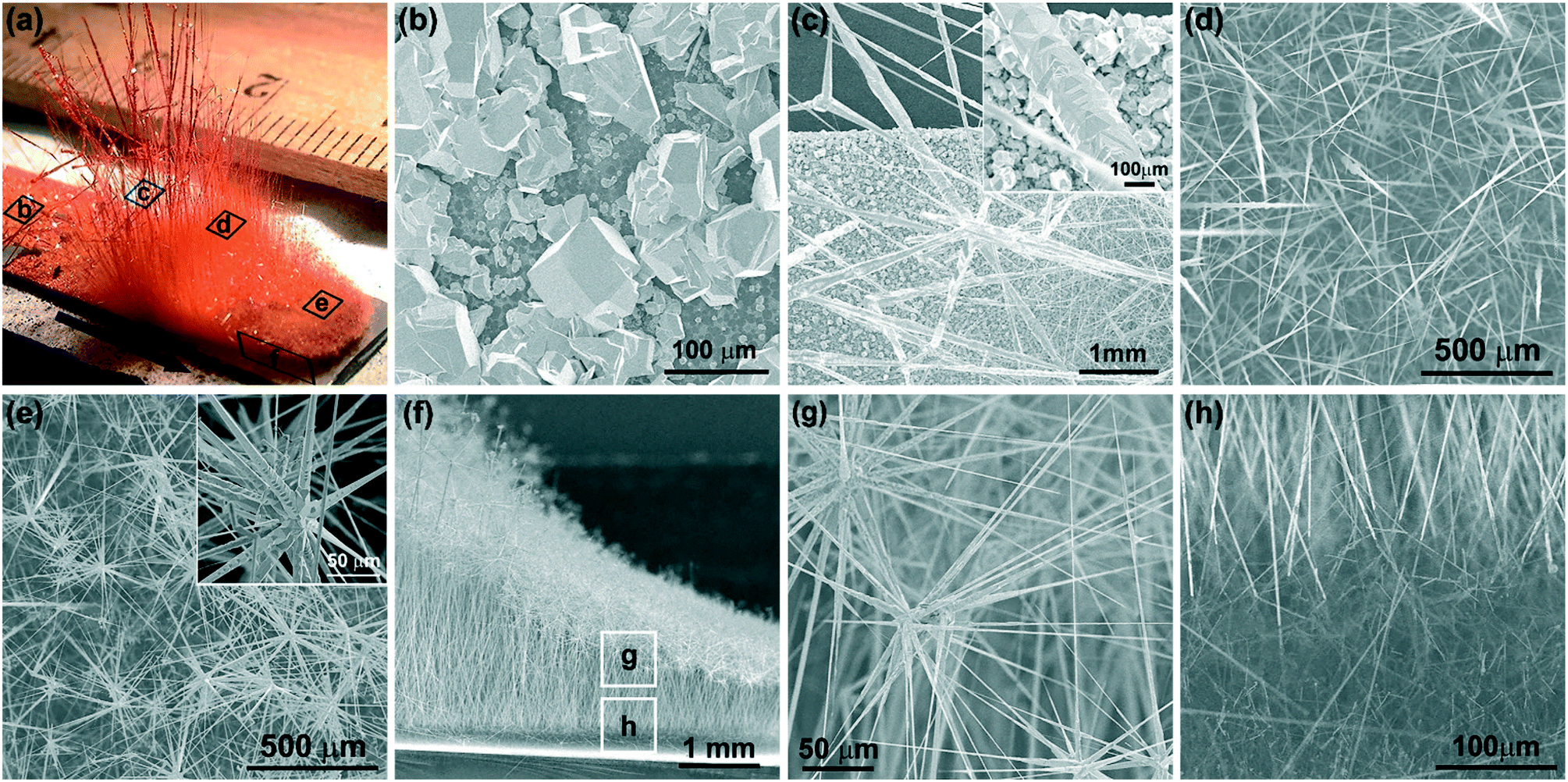 | ||
| Fig. 1 CVD growth of ZnTe nanostructures. (a) Photo of the ZnTe deposition overview on the substrate showing morphological changes of different growth zones as the growth temperature decreases along the flow direction (indicated by the arrow). (b–e) Top-view SEM images of the ZnTe growth zones at different locations as labeled in (a): (b) islands, (c) ultra-long microwires with the inset of the high-magnification image showing surface facets, (d) straight nanowires, and (e) branched nanowires with the inset of the branched tips. Side-view (f) low-magnification SEM image of the branched nanowires and high-magnification images showing the (g) top layer and (h) bottom layer. | ||
The composition of the deposits was determined using EDS in SEM. Fig. 2 shows typical results from the stem of microwires (Fig. 2a) and the tip of branched nanowires (Fig. 2b). From the microwires, the EDS spectrum (Fig. 2c, bottom spectrum) shows strong Te and Zn peaks with a negligible O signal probably due to slight surface oxidation. The ratio of atomic percentages between Zn and Te is 50.96![[thin space (1/6-em)]](https://www.rsc.org/images/entities/char_2009.gif) :49.04 ≈ 1.04:1, very close to the 1:1 stoichiometry of ZnTe. However, at the tip of the branched nanowires (Fig. 2c, top spectrum), a strong Si peak is found besides the Zn and Te signals. Careful examination was performed on multiple locations of the branched nanowires. The strong Si signal only showed up at the tips, while no Si signal was found from the stems of the nanowires. The Si peak at the tips of the branched ZnTe nanowires is not from the background Si substrate and its origin will be discussed later in the text. The crystallinity of the deposits was confirmed by XRD (Fig. 2d), with diffraction peaks matching closely with the standard pattern of the cubic zincblende ZnTe phase (ICDD PDF # 00-015-0746, a = 6.1026 Å). The growth of the ZnTe micro- and nanostructures is similar to that of the previous report.9 The growth mechanism is dominated by the VLS growth with Au particles as the catalysts promoting the axial growth, while the vapor–solid growth accounts for the radial growth resulting in the thick diameter of the microwires and the tapered growth of the nanowires.9 The ZnTe growths at different growth pressures from 20 Torr to 200 Torr were explored. The growth yield of ZnTe reached its highest at a growth pressure of ∼50 Torr, and it became lower when the growth pressure was away from 50 Torr. More interestingly, un-expected jellyfish-like nanostructures (Fig. 2e–h) were found among the ZnTe deposits when the ZnTe yield was low. These nanostructures appeared among the ZnTe deposits with a low density. Their growth locations varied randomly across the whole substrate in different experiments, i.e., in the growth, they could appear at some zones among the growth zones b–e shown in Fig. 1. Despite the detailed differences in morphology, these nanostructures all have large particles on top of the tentacle-like tiny nanowires with diameters of a few nanometers and lengths up to tens of microns. It is important to figure out what materials these nanostructures are and how they formed during the ZnTe growth. Therefore, the focus of this report is centered on exploring the growth mechanism of this unexpected growth of nanostructures and revealing the detailed atomic processes during the nanostructure formation.
:49.04 ≈ 1.04:1, very close to the 1:1 stoichiometry of ZnTe. However, at the tip of the branched nanowires (Fig. 2c, top spectrum), a strong Si peak is found besides the Zn and Te signals. Careful examination was performed on multiple locations of the branched nanowires. The strong Si signal only showed up at the tips, while no Si signal was found from the stems of the nanowires. The Si peak at the tips of the branched ZnTe nanowires is not from the background Si substrate and its origin will be discussed later in the text. The crystallinity of the deposits was confirmed by XRD (Fig. 2d), with diffraction peaks matching closely with the standard pattern of the cubic zincblende ZnTe phase (ICDD PDF # 00-015-0746, a = 6.1026 Å). The growth of the ZnTe micro- and nanostructures is similar to that of the previous report.9 The growth mechanism is dominated by the VLS growth with Au particles as the catalysts promoting the axial growth, while the vapor–solid growth accounts for the radial growth resulting in the thick diameter of the microwires and the tapered growth of the nanowires.9 The ZnTe growths at different growth pressures from 20 Torr to 200 Torr were explored. The growth yield of ZnTe reached its highest at a growth pressure of ∼50 Torr, and it became lower when the growth pressure was away from 50 Torr. More interestingly, un-expected jellyfish-like nanostructures (Fig. 2e–h) were found among the ZnTe deposits when the ZnTe yield was low. These nanostructures appeared among the ZnTe deposits with a low density. Their growth locations varied randomly across the whole substrate in different experiments, i.e., in the growth, they could appear at some zones among the growth zones b–e shown in Fig. 1. Despite the detailed differences in morphology, these nanostructures all have large particles on top of the tentacle-like tiny nanowires with diameters of a few nanometers and lengths up to tens of microns. It is important to figure out what materials these nanostructures are and how they formed during the ZnTe growth. Therefore, the focus of this report is centered on exploring the growth mechanism of this unexpected growth of nanostructures and revealing the detailed atomic processes during the nanostructure formation.
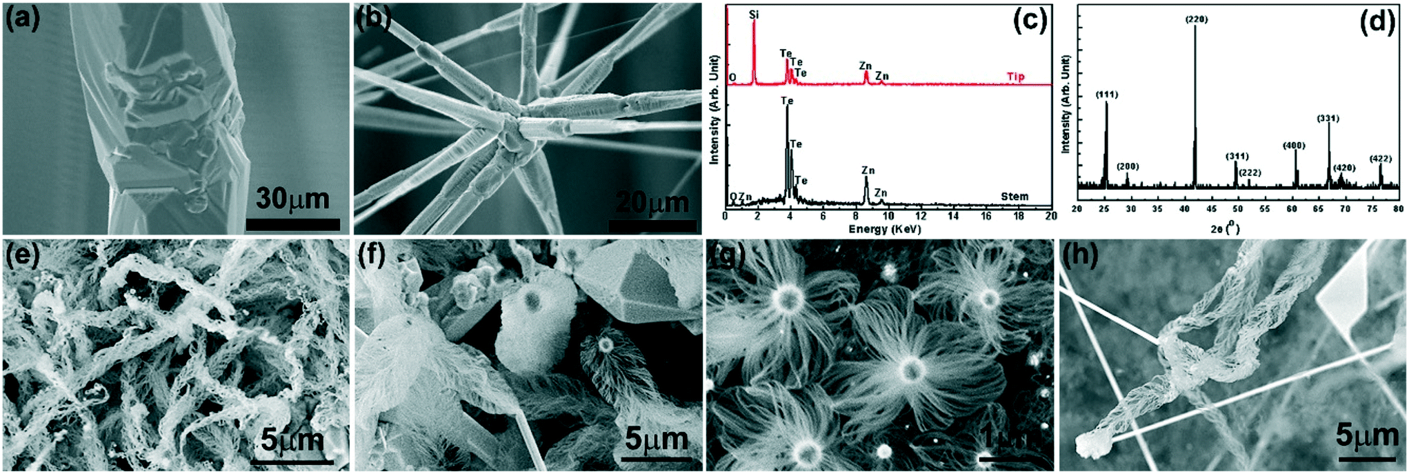 | ||
| Fig. 2 SEM images of the (a) stem of a ZnTe microwire and (b) tip of a branched nanowire, (c) corresponding EDS spectra for (a) and (b), and (d) XRD spectrum of the ZnTe deposits. (e–h) SEM images of different jellyfish-like nanostructures. | ||
A series of control experiments have been performed to investigate the growth mechanism of these jellyfish-like nanostructures. One experiment was carried out without any source materials. Only an Au-coated Si substrate was loaded with all the other growth parameters kept the same as those for the typical ZnTe growth. As shown in Fig. 3a, no nanostructures were found except the gold nanoparticles on the substrate surface. The gold nanoparticles formed due to the thermal annealing of the Au coating during the growth. This result rules out the possibility that these nanostructures could be induced by the Au catalyst alone on the substrate under the growth conditions employed in this study. Therefore, the growth of the jellyfish-like nanostructures must be related to the by-products from the ZnTe source. During the ZnTe growth, the ZnTe source could sublimate and react with H2, producing a variety of reaction intermediates in the vapor phase including ZnTe, Zn, Te, Te2, H2Te, etc.10 First, the role of Zn vapor was identified by an experiment using Zn powders as the source materials. The Zn powders were located upstream at ∼300 °C producing a vapor pressure of ∼1.45 mTorr.11 As shown in Fig. 3b, only the tiny Au particles were found on the substrate showing that the Zn vapor could not induce the nanostructure growth. The resulting Au particles are smaller than those particles in Fig. 3a probably due to the dissolution of Zn into the Au particles.
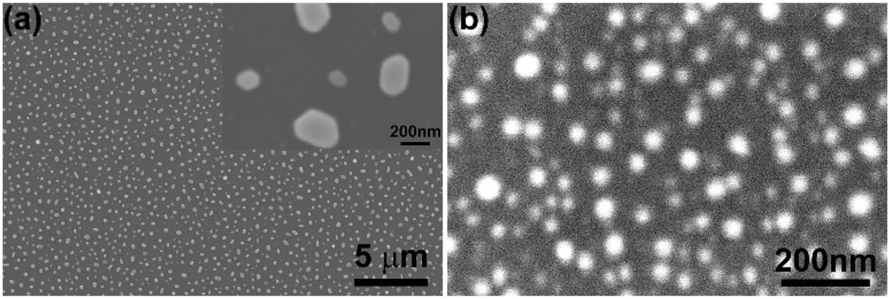 | ||
| Fig. 3 SEM images of the substrates after (a) the growth without any source material and (b) the growth using Zn powders as the source material. Both growths show only the Au particles on the surface. | ||
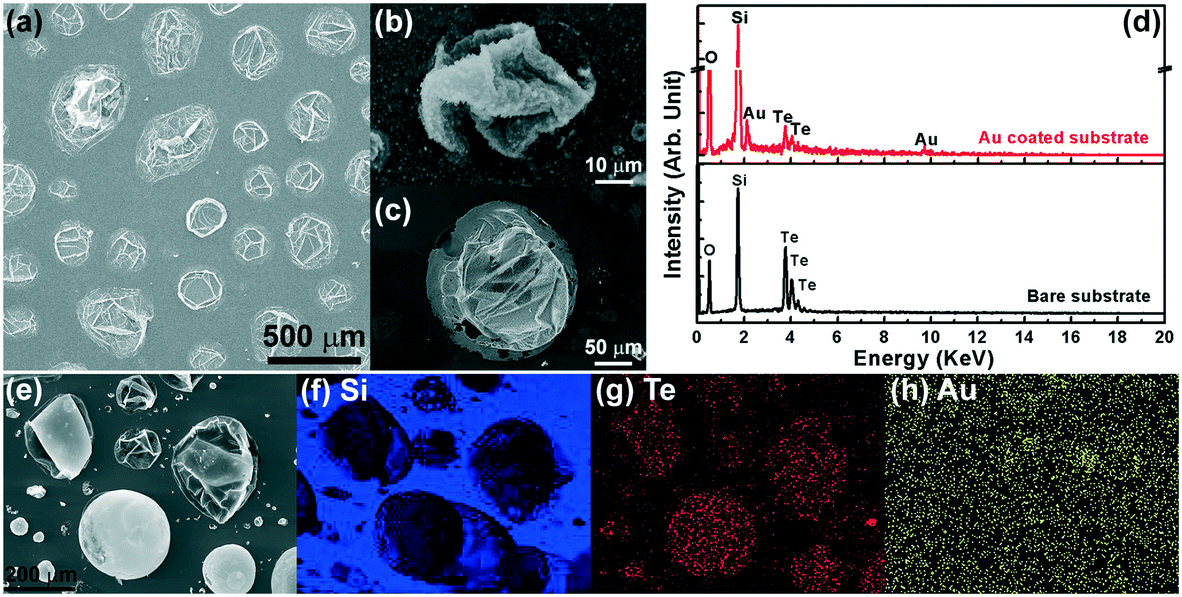
Next, Te powders were used as the source material to verify the effects of Te-based species in the nanostructure growth. The Te powders were located upstream at ∼670 °C with a vapor pressure of ∼16.7 Torr.12 The nanostructures with different morphologies were found on the substrate, as shown in Fig. 4. The high density of the jellyfish-like nanostructures was obtained in a growth zone with a growth temperature from ∼758 °C (Fig. 4a) to ∼624 °C (Fig. 4b). Beyond this growth zone with higher growth temperature upstream (∼812–758 °C), the nanostructures quickly become shorter and disappear. At downstream locations along the substrate, the deposit gradually morphs into thick nanowires at ∼612 °C (Fig. 4c), short nanorods at ∼600 °C (Fig. 4d), and nanospheres at ∼565 °C (Fig. 4e). All the jellyfish-like nanostructures have ball-shaped catalyst particles on top of the dense and long nanowire tentacles. On the other hand, most of the thick nanowires shown in Fig. 4c have a structure with a single nanowire beneath each catalyst particle. This morphology change can be attributed to the lower growth temperature that promotes the bundling and merging of thin nanowire tentacles forming one thick nanowire. The formation of nanorods and nanospheres downstream is due to the further decrease of growth temperature and the reduction of vapor supplies. The nanorods have a mushroom-like structure with a large catalyst top above a short and thick stem, while the nanospheres exhibit a core–shell structure with the deposit wrapping outside the catalyst particle. EDS analyses (Fig. 4f) were performed at different locations. All the nanostructures have large signals of Si and O indicating the deposition of SiOx, while the Au signals are from the Au catalysts. It is worth mentioning that no Te signals are found for all the nanowires (Fig. 4f, top spectrum), both the jellyfish-like and the thick ones, while the Te signals are clearly present in the nanorods (Fig. 4f, middle) and nanospheres (Fig. 4f, bottom). This result indicates that the Te content is lower than the detection limit of EDS in the nanowires grown at high temperature (above ∼612 °C), while more Te content is able to form in nanorods and nanospheres due to their lower growth temperature (∼600–565 °C).
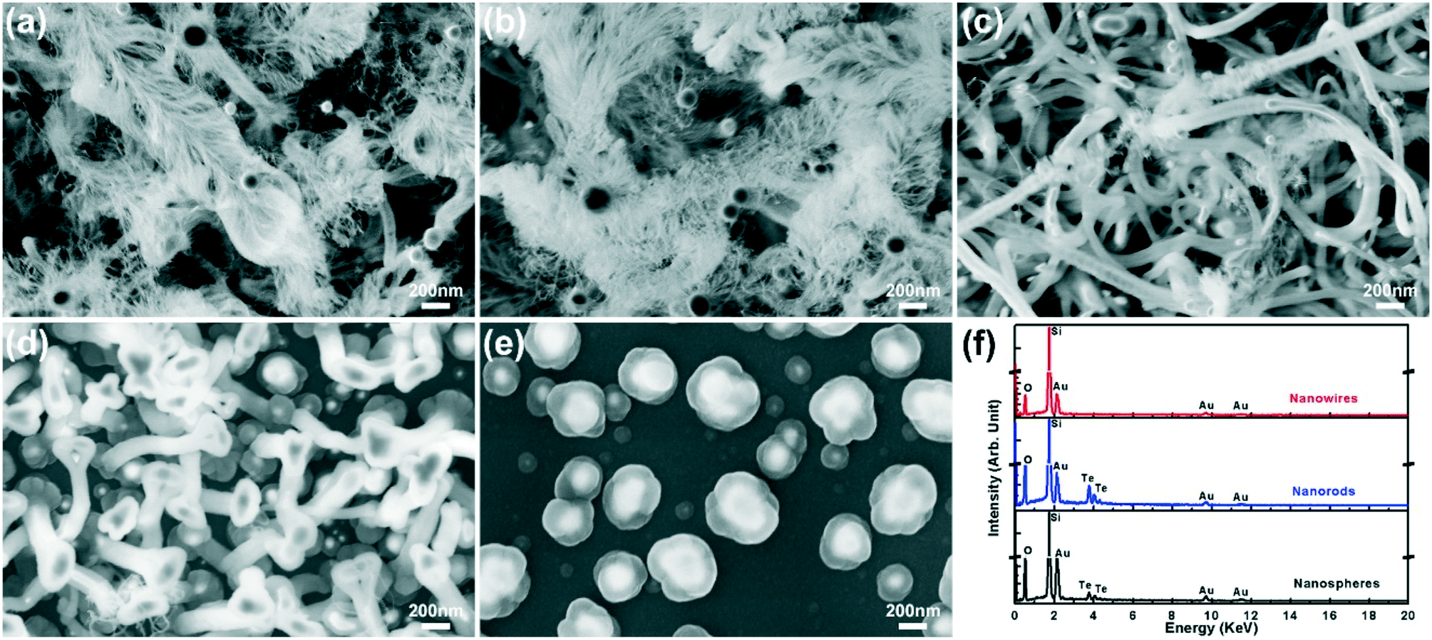 | ||
| Fig. 4 SEM images of the SiOx nanostructures at different growth temperatures: (a and b) jellyfish-like thin nanowires, (c) thick nanowires, (d) mushroom-like nanorods, and (e) core–shell nanospheres. (f) Corresponding EDS spectra of the deposits with different morphologies. | ||
Since the Si and O signals could also come from the background of the Si substrate, TEM analyses were performed on the nanostructures to further confirm their composition and identify their structures. Study has been mainly focused on the jellyfish-like nanowires and the results are shown in Fig. 5. Fig. 5a shows a typical jellyfish-like nanostructure with lots of nanowire tentacles attached to one large catalyst particle. Fig. 5b shows a nanostructure with only one straight nanowire attached to the particle, but it is also possible that other nanowire tentacles were lost during the sample transferring from the substrate to the TEM grid. Fig. 5c shows a similar jellyfish-like nanostructure, but the nanowire tentacles have a nodular morphology. All the tentacle nanowires are very thin with only a few nanometers in diameter, while the catalyst particles are larger, about 100–200 nm in diameter. The insets in Fig. 5a and b show the catalyst–nanowire interfaces and some branched structures between the nanowires. It should be emphasized that the jellyfish-like nanostructures have a significantly different catalyst–nanowire interface from the one for the classic VLS growth. For the conventional VLS growth, there is a sharp and straight interface between the catalyst and the nanowire. However, for the jellyfish-like nanostructures, the whole catalyst particle is wrapped in a thin layer of deposits and the tentacle nanowires are grown on this shell layer of deposits. From the EDS analyses (Fig. 5d), the nanowires can be identified as the SiOx nanowires with strong signals of Si and O, while the catalyst particle is Au alloyed with Si with a thin shell of SiOx (please note that the additional Cu, Cr, and C signals are background signals from the TEM column and the sample grid). Again, no Te signals were detected in these jellyfish-like nanostructures, either from the nanowires or from the catalyst particles.
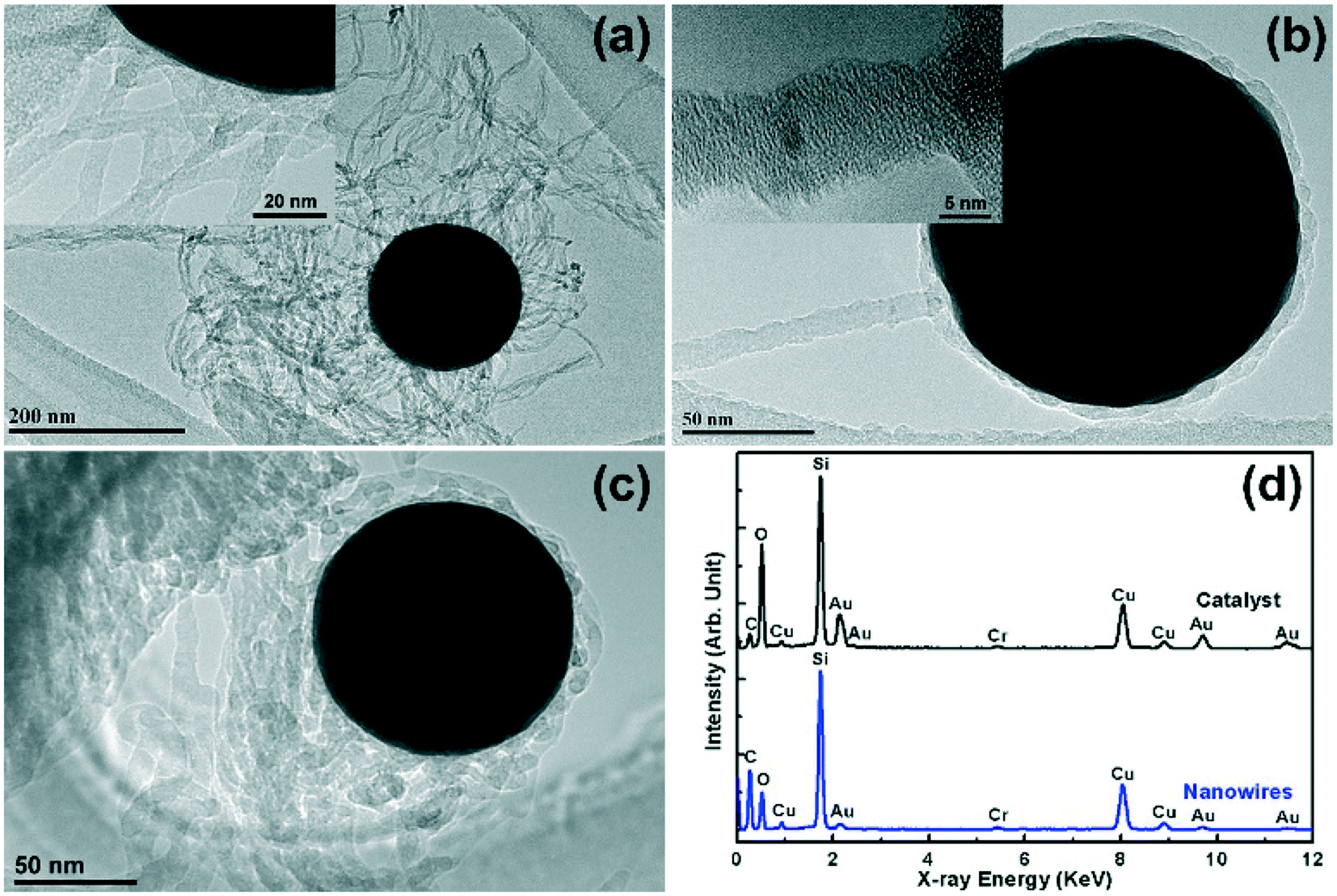 | ||
| Fig. 5 (a–c) TEM images of typical jellyfish-like SiOx nanowires with insets showing the structures at the nanowire–catalyst interface, and (d) EDS spectra of the catalyst (top) and nanowires (bottom). | ||
Questions arise based on the above analyses. Why is the Te source required to induce the growth of the jellyfish-like nanostructures while no Te was detected in the nanostructures? What is the role of Te in the nanostructure growth? And what are the differences between the functions of Te and Au in the nanostructure growth? To answer these questions and to reveal the growth mechanism of the nanostructures, growth processes have been analyzed in detail. First, from the SEM and TEM analyses, it is easy to identify that the Au particles on top of the nanowires serve as the catalysts promoting the nanowire growth, similar to the conventional VLS growth. The growth was performed using the Te source without the Au coating on the substrate, and no deposit was found on the substrate. This result further verifies the function of Au as the catalysts for the VLS growth of the nanostructures. Au is a common catalyst for the VLS growth of Si nanostructures, as the Au–Si system forms a eutectic at 363 ± 3 °C with a eutectic composition of 18.6 ± 0.5 at% Si.13 Si vapor dissolves into the Au forming eutectic liquid droplets. When the Si content reaches beyond its solubility limit in Au, it will precipitate inducing the nanostructure growth.
Therefore, it is essential to answer how the Si vapor was produced during the growth as no Si precursor was introduced into the CVD system except the Si substrate. Considering the experimental facts that the SiOx nanostructures could not be produced without ZnTe or Te sources, we propose a hypothesis that Te-based vapors can react with solid Si and produce Si vapor for the nanostructure growth. The Si–Te phase diagram shows that Te can react with Si forming the compound Si2Te3, which then forms a eutectic with Te (i.e., L ⇌ Si2Te3 + Te) at 406 °C with a composition of 82.5 at% Te (i.e., 17.5 at% Si).14 Hence, it is possible that Te can induce Si vapor during the growth assisting the formation of the SiOx nanostructures. To prove this theory, experiments were carried out with the Te source heated at 850 °C, where the Te vapor pressure can reach to ∼2 × 10² Torr (note: this is the saturated pressure at equilibrium. The total growth pressure was still maintained at 50 Torr with vacuum pumping).12 As shown in Fig. 6a, large bubble-like particles formed on the Si substrate surface due to the large amount of Te vapors produced at the high heating temperature. The particles etched deeply into the Si substrate and they could form on either the bare Si substrate (Fig. 6b) or Au-coated Si substrate (Fig. 6c). These results prove that Te vapors can react with Si substrate forming eutectic particles on the substrate. The corresponding EDS results in Fig. 6d confirm that the composition of the particles are mainly Si and Te, with O from oxidation and Au for the Au-coated substrate. All the bubble-like particles have a similar morphology with empty cores and most of them have a wrinkled surface morphology. The bubble-like morphology indicates that the eutectic droplets are not stable during the growth. The Te content will be re-evaporated, therefore release Si vapor. This phenomenon produces particles like bubbles blown up by the vapors. After the growth completes and the system is cooled down, some bubbles shrink forming the wrinkled surfaces and some bubbles keep their round shapes probably due to their higher thickness. This analysis also explains why the Te signals were not found in all the bubble-like particles in the EDS measurement. Some bubble-like particles have no significant Te signals due to the depletion of the Te content during the growth. Fig. 6e and f show the EDS elemental mapping of these Si–Te eutectic particles on an Au-coated Si substrate. The mapping shows that the Si signal is present everywhere throughout the substrate (Fig. 6f) but its intensity becomes lower at the locations of these bubble-like particles, while the Te signal (Fig. 6g) is only from these bubble-like particles. This result confirms that the bubble-like particles were formed from the Te vapor that reacted with the Si substrate, and the low intensity of the Te signal indicating the consumption of Te during the growth. Due to the thin thickness (10 nm) of the Au coating on the substrate, the Au signal for mapping shown in Fig. 6h is very low, mostly from the background noises. The EDS mapping of the particles on a bare Si substrate (not shown) was also performed, which is similar to the result shown in Fig. 6f and g just without the Au signal.
 | ||
| Fig. 6 SEM images of (a) Si–Te eutectic particles formed on the Si substrate and individual particles on (b) Au-coated Si and (c) bare Si substrate. Corresponding EDS spectra of (d) the Si–Te eutectic particles. Elemental mapping of the Si–Te eutectic particles with (e) the SEM image and corresponding EDS signals of (f) Si, (g) Te, and (h) Au, respectively. | ||
Now, the different roles of Te and Au in the SiOx nanostructure growth are clear. As they both can form eutectics with Si, Te will induce the production of Si-based vapor, while Au will promote the SiOx nanostructure growth through the VLS mechanism. The stability theory of catalysts can successfully explain why Au and Te behave differently in the growth of the SiOx nanostructures. Au has very low vapor pressure even at elevated temperatures, for example, the Au vapor pressure is about 1.09 × 10⁻⁵ Torr at its melting temperature Tm = 1046 °C.15 Therefore, the Au catalysts are very stable at the substrate heating temperature (∼812–565 °C) with negligible vapor pressure. As a result, Au can serve as catalysts promoting the nanostructure growth, but it cannot produce the Si precursor for the growth under the given experimental conditions. In contrast, the Te catalysts are not stable with a low melting temperature at 450 °C. The vapor pressure of Te at 615 °C already reaches 7.5 Torr, much higher than the one for Au.12 This fact explains why there were no Te signals in the SiOx nanowires grown above ∼612 °C, while a small amount of Te was found in nanorods and nanospheres at ∼600–565 °C. Because of its high vapor pressure, the Te vapors produced from the source materials react with the Si substrate at high temperature zone forming eutectic particles, which are subsequently re-evaporated releasing the Si vapor for the growth of the SiOx nanostructures at lower temperature zones. Therefore, during the ZnTe growth, the Si source was induced by the intermediate Te species, such as Te, Te2, H2Te, etc. The Si contents in the deposits are affected by the dynamics of different reactions during the growth. In the typical ZnTe growth at 50 Torr with high yield of the ZnTe nanostructures shown in Fig. 1, the Zn species and Te species were balanced. The reaction between the Te vapors with the Si substrate was negligible, as the ZnTe formation from the Zn and Te species was dominant. This analysis explains why the Si content was not found in the majority of the ZnTe deposits in our growth and previous report.9 However, the Si signals were present at the tips of the branched ZnTe nanowires. This result can be attributed to the changes in reaction dynamics during the cooling stage. As the heating temperature decreased, the balance between the Zn and Te species shifted and promoted the Te–Si reactions to produce Si vapor. The Si vapor was accommodated into the deposits at the tips of the ZnTe nanowires at low growth temperature and this was possibly the reason for the formation of the branched nanostructures. When growth conditions changed with growth pressures different from 50 Torr, growth dynamics could change a lot resulting in enhanced Te–Si reactions during the growth stage. This change explains the lower yield of ZnTe deposits and the appearance of more SiOx nanostructures. Y. L. Chao et al. reported the growth of ZnTe–SiOx core–shell nanostructures using slightly different growth conditions.10a They concluded that the Au coating on the first Si substrate at high temperature of 1040 °C was responsible for the evaporation of Si substrate forming the SiOx shells. However, our results indicate that the role of intermediate Te species may not be ignored in the production of Si vapor. Although no SiOx shells formed without the Au coating on the Si source substrate in their control experiment, it might be due to the high heating temperature of 1040 °C for the Si source substrate at the center of the furnace. The chance was low for Te vapors to adsorb onto the Si substrate and react at such high heating temperature, but the presence of Au could possibly incorporate the Te species forming Au–Te–Si eutectics and producing Si through re-evaporation. Additional experiments without the ZnTe source may help to clarify the details.
Based on all the experimental results and the mechanism analyses, we propose the growth mechanism of the SiOx nanostructures with detailed atomic processes as demonstrated in Fig. 7. In the source zone (Fig. 7a), the ZnTe source sublimates and reacts with H2 producing various Te-based intermediates (e.g., Te, Te2, H2Te, etc.). Similar processes occur if the source is replaced by the Te powders. The Te-based vapors are transferred downstream. They will first interact with the Si substrate at high temperature end (∼812–758 °C), i.e., the Si-vapor production zone (Fig. 7b). The Te species react with Si on the surface forming eutectic particles, which may also contain Au from the Au coating on the substrate (Fig. 7b-I). Due to the instability of the Te–Si eutectic particles, the particles evaporate and release Te and Si vapors into the reaction chamber (Fig. 7b-II). The Si vapor induced by the Te species becomes the source for the SiOx nanostructure formation on the substrate at lower temperature end, i.e., the nanostructure growth zone (Fig. 7c). The SiOx nanostructures form on the substrate with different morphologies, including jellyfish-like nanowires (Fig. 7c-II), thick nanowires (Fig. 7c-III), nanorods (Fig. 7c-IV), and nanospheres (Fig. 7c-V). The nanostructure formation follows the VLS mechanism. The formation of SiOx might be due to the residual O2 in the reaction chamber. However, the resulting nanostructures were most probably amorphous Si under the reduction growth conditions provided by the H2 flow. The amorphous Si nanostructures were subsequently oxidized into SiOx when they were exposed to the air after the growth. Different from the conventional VLS nanostructures, the formation of the jellyfish-like nanowires is discussed here in detail. The evolution of the jellyfish-like nanowires with growth time is schematically demonstrated in Fig. 7c-I. The nanostructure growth is promoted by the Au catalysts, which form eutectic particles with Si vapor in the growth zone. The round-shaped particles indicate that the catalysts are liquid droplets during the growth. In the classic VLS growth, after the catalysts are saturated with the source materials, the deposit precipitates out of the catalysts forming a sharp straight liquid–solid interface. This liquid–solid interface will then serve as the growth front guiding the growth of nanowires. However, as revealed by the TEM results (Fig. 5), in our experiments, Si will precipitate all over the surface of the saturated Au catalysts forming the shells of amorphous Si outside the catalysts. During the growth, the continuous supply of Si will diffuse along the surface of the amorphous Si shells, nucleate and form first a few nanowires. As the nanowires grow longer, the core–shell catalysts are lifted up. More nucleation events can happen on the surface of the Si shells forming more nanowires. The multiple nucleation sites on the surface of the Si shells result in the jellyfish-like nanostructures with many nanowire tentacles. The nanowire nucleation could also occur on the surface of the existing nanowires forming the branched nanowires. Nanowires can curve during the growth producing twisted nanostructures. Schematic drawings of these typical nanowires are demonstrated in Fig. 7c-II. It is worth noting that in the conventional VLS growth, each catalyst particle can only induce one nanowire dictating the shape and dimension of the nanowire. For the growth of the jellyfish-like nanostructures in this report, one large catalyst particle induces the growth of many nanowires. Therefore, the shape and dimension of these nanowires are not controlled by the dimension of the catalyst particles. They are most probably controlled by the dimension of the nucleation sites on the Si shells of the catalysts. With the decrease of the growth temperature downstream, the surface diffusion of Si decreases promoting faster nucleation. Together with the reduced Si-based vapor supply to downstream, the nanostructures grow thicker and shorter producing thick nanowires, nanorods, and nanospheres (Fig. 7c-III–V).
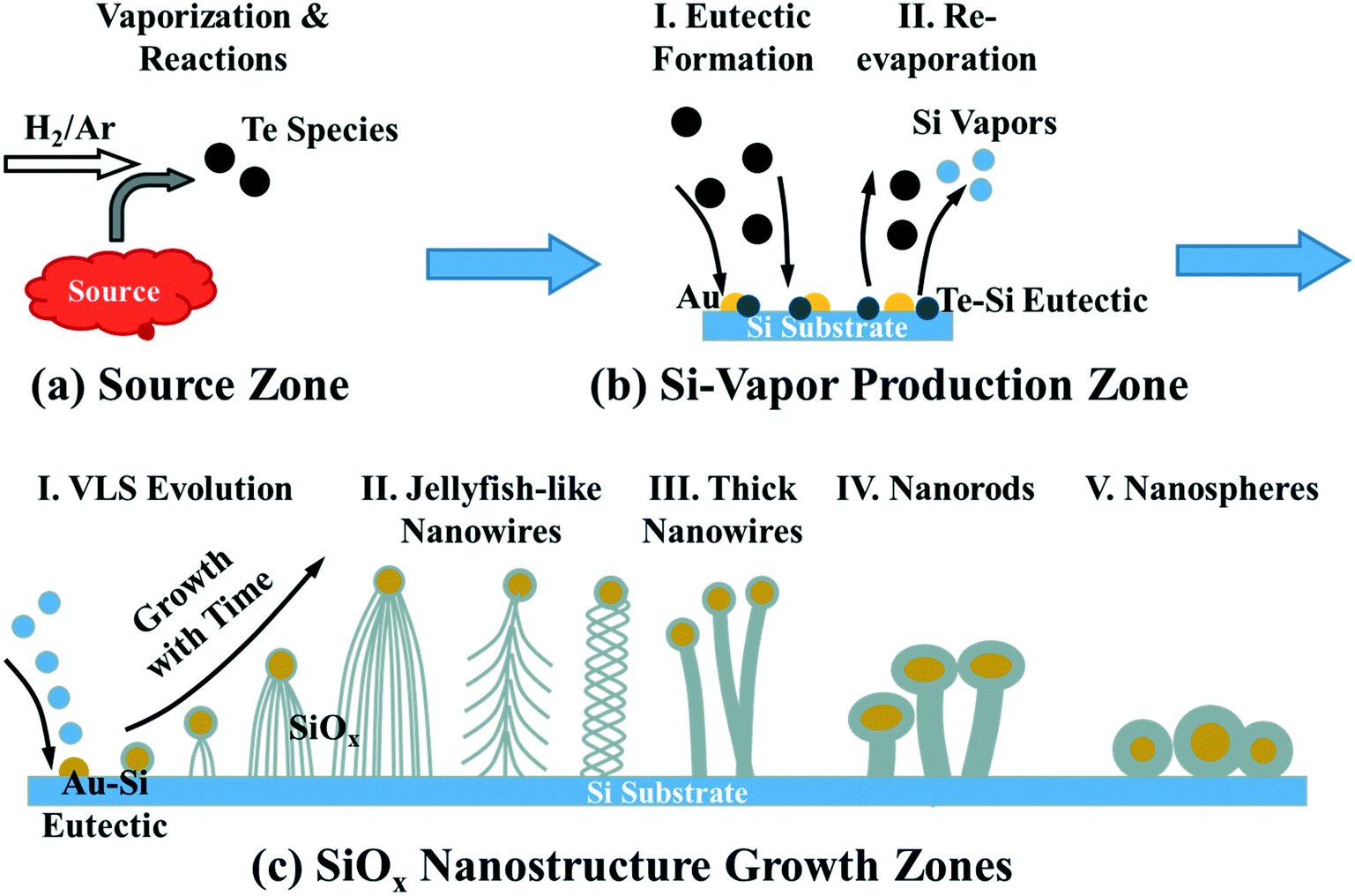 | ||
| Fig. 7 Schematics of the growth mechanism and physical processes of the SiOx nanostructures: (a) source zone produces Te-based species, (b) Si-vapor production zone on the Si substrate at high temperature end, and (c) growth zones of the SiOx nanostructures on the Si substrate at lower substrate temperature. | ||
As discussed above, the Si vapor was not supplied intentionally for the growth of the SiOx nanostructures in our experiments. It was induced by the reaction intermediates of Te-based species. Therefore, it deserves to make a comparison with other reports of the SiOx nanostructures with similar morphologies. This comparison will help us to have a better understanding of the growth mechanism and atomic processes during the growth. Table 1 lists some typical reports on the growth of SiOx nanostructures with similar morphologies. The majority of the previous reports have employed Si precursors to produce Si-based vapors and catalysts to promote the nanostructure growth. Z. W. Pan et al. first reported the growth of similar amorphous SiOx nanostructures induced by the Ga droplets from GaN decomposition.5b The Ga droplets served two roles in their report: (1) producing Si vapor by etching the Si substrate and releasing Si at high temperature and (2) promoting the SiOx growth as the catalysts at low temperature. In their later report, the Si source was replaced by SiH4 without the need of assistance of the Ga droplets.16 Many groups employed SiO as the Si source for the growth by evaporating SiO powders or by oxidizing and evaporating Si in a residual O2 environment.17 Mechanism investigations have shown that the volatile SiO species produced from high temperature annealing of Si with low residual O2 contents are the essential precursors for the growth of SiOx nanostructures.18 Some claimed direct evaporation of the Si substrate or powders to produce Si vapor for the growth,19 however, the formation and evaporation of SiO could not be ruled out due to the presence of the residual O2. In these reports, residual O2 or air leakage was responsible for the formation of SiOx and different types of metal catalysts were used to promote the growth of the SiOx nanostructures. In this work, the formation of the SiOx nanostructures was discovered among the ZnTe growth without intentionally introducing the Si source. Two elements played different roles important to the SiOx growth: the intermediate Te-based species from the ZnTe induced the Si source by dissolving the Si substrate and releasing Si vapor, while Au served as the catalysts to promote the nanostructure growth. Therefore, this phenomenon is important for the composition and phase control in the growth of compound nanostructures in which by-products may be induced by reaction intermediates. Based on the unveiled growth mechanism, the experiments were modified to the high-yield growth of the SiOx nanostructures by using the Te powders as the source materials. Compared to other reports, this result provides a convenient and low-cost method with much lower heating and growth temperatures, as summarized in Table 1. This work can be further developed to become “greener” and more cost-efficient. For example, using Te as a transport agent, Si vapor can be produced directly from low-cost Si powders for the growth of different Si-based nanostructures without using those expensive and hazardous precursors (e.g., SiH4). Other elements that can form eutectics with Si and subsequently evaporate to release the Si vapor could also be searched. It is possible to employ inexpensive catalysts, such as Cu, to replace expensive Au to promote the nanostructure growth. Crystalline nanostructures could also be produced by adjusting the growth temperature and other growth parameters.
| Ref. | Si source | VLS catalysts | Heating temperature | Growth temperature |
|---|---|---|---|---|
| Z. W. Pan et al., 2002 (ref. 5b) | Si etching and releasing by Ga (from GaN decomposition) | Ga from GaN decomposition | 1150 °C | 1000–850 °C |
| Z. W. Pan et al., 2003 (ref. 16) | SiH4 | Ga from GaN decomposition | 1150 °C | 1100–950 °C |
| C. L. Pang et al., 2011 (ref. 17a) | SiO powders | Ge powders | 1600 °C | 1600 °C |
| M. N. Banis et al., 2011 (ref. 17b) | SiO from Si + residual O2 | VO2 and Au | 1000 °C | 1000 °C |
| J. Y. Qu et al., 2012 (ref. 17c) | SiO from Si + residual O2 and/or SiClx from Si + HCl | Fe from FeCl3 + H2 | 1000–1200 °C | 1000–1200 °C |
| R. G. Elliman et al., 2012 (ref. 17d) | SiO from Si + O2 impurity (enhanced by Au) | Au | 1100 °C | 1100 °C |
| A. Gomez-Martinez et al., 2016 (ref. 17e) | SiO from Si + residual O2 | Au (on Si substrate) or Cu foil | 900 °C | 900 °C |
| Z. D. Xiao et al., 2006 (ref. 19a) | Si substrate | Sn from SnO2 + C | 1150 °C | 500 °C |
| R. B. Wu et al., 2007 (ref. 19b) | Si powders | Fe | 1500 °C | 1500 °C |
| This work | Si dissolving and releasing by Te species (from ZnTe + H2) | Au | 850 °C | 758–565 °C |
4 Conclusions
In summary, the SiOx nanostructures discovered in the ZnTe growth were induced by the reaction intermediates, Te-based species. Growth mechanism study and analysis have revealed the different roles of the Te species and Au catalyst in the SiOx nanostructure growth. The Te species dissolve the Si substrate by forming a eutectic and then release Si vapor through subsequent evaporation. Meanwhile, the Au catalysts accommodate the Si vapor to promote the growth. With the unique core–shell Au–Si catalyst structures, amorphous SiOx nanostructures can form at different growth temperatures with various morphologies, including jellyfish-like nanowires, thick nanowires, nanorods, and nanospheres. This result indicates the importance of composition and phase control in the growth of compound nanostructures. Complicated intermediates might introduce unexpected compositions and even different phases into the deposits. This study also provides a new method for the SiOx nanostructures with low growth temperature and low cost without using expensive and hazardous precursors. The new growth mode could be further developed into the low-cost high-efficiency growth of the 1D nanostructures of other materials.Conflicts of interest
The authors declare no competing financial interest.Acknowledgements
This work was supported by the National Science Foundation (NSF) under grant DMR-1006547, the start-up fund from the Department of Mechanical Engineering and Engineering Science (MEES), the Charlotte Research Institute at the University of North Carolina at Charlotte (UNC Charlotte), and the faculty research grant from UNC Charlotte. The authors acknowledge the Department of MEES and the Center for Optoelectronics and Optical Communications at UNC Charlotte for the use of multi-user facilities. T. S. acknowledges the financial support from the NSF DMR-1006547 and the teaching assistantship from the Optical Science and Engineering Program at UNC Charlotte. J. J. H. and E. O. acknowledge the Research Experience for Undergraduate (REU) supports from the NSF DMR-1006547 and the MEES Summer REU program.Notes and references
- Y. N. Xia, P. D. Yang, Y. G. Sun, Y. Y. Wu, B. Mayers, B. Gates, Y. D. Yin, F. Kim and Y. Q. Yan, Adv. Mater., 2003, 15, 353–389 CrossRef CAS
.
- M. Law, J. Goldberger and P. D. Yang, Annu. Rev. Mater. Res., 2004, 34, 83–122 CrossRef CAS
- Y. Y. Wu and P. D. Yang, J. Am. Chem. Soc., 2001, 123, 3165–3166 CrossRef CAS
-
(a) H. J. Fan, P. Werner and M. Zacharias, Small, 2006, 2, 700–717 CrossRef CAS PubMed
-
(a) H. Chandrasekaran, G. U. Sumanasekara and M. K. Sunkara, J. Phys. Chem. B, 2006, 110, 18351–18357 CrossRef CAS PubMed
- Z. W. Pan, S. Dai, C. M. Rouleau and D. H. Lowndes, Angew. Chem., Int. Ed., 2005, 44, 274–278 CrossRef CAS PubMed
-
(a) J. Wang, K. Chen, M. Gong, B. Xu and Q. Yang, Nano Lett., 2013, 3996–4000 CrossRef CAS PubMed
-
(a) H. T. Zhang, T. T. Xu, M. Z. Tang, T. H. Her and S. Y. Li, J. Vac. Sci. Technol., B, 2010, 28, 310–315 CrossRef CAS
- M. I. B. Utama, M. de la Mata, Q. Zhang, C. Magen, J. Arbiol and Q. Xiong, Cryst. Growth Des., 2013, 13, 2590–2596 CrossRef CAS
-
(a) Y. L. Cao, Y. B. Tang, Y. Liu, Z. T. Liu, L. B. Luo, Z. B. He, J. S. Jie, R. Vellaisamy, W. J. Zhang, C. S. Lee and S. T. Lee, Nanotechnology, 2009, 20, 455702 CrossRef CAS PubMed
-
CRC Handbook of Chemistry and Physics, ed. D. R. Lide, CRC Press, Boca Raton, Florida, 2003 Search PubMed
- National Physical Laboratory, Kaye and Laby Tables of Physical and Chemical Constants, http://www.kayelaby.npl.co.uk/, Accessed May, 2018, 2018
- H. Okamoto and T. B. Massalski, Bull. Alloy Phase Diagrams, 1983, 4, 190–198 CrossRef
- B. Legendre, C. Souleau, C. Hancheng and N. Rodier, J. Chem. Res., 1978, 168–169 CAS
- C. B. Alcock, V. P. Itkin and M. K. Horrigan, Can. Metall. Q., 1984, 23, 309–313 CrossRef CAS
- Z. W. Pan, S. Dai, D. B. Beach and D. H. Lowndes, Nano Lett., 2003, 3, 1279–1284 CrossRef CAS
-
(a) C. L. Pang, H. Cui and C. X. Wang, CrystEngComm, 2011, 13, 4082–4085 RSC
-
(a) A. Gomez-Martinez, F. Marquez and C. Morant, Appl. Surf. Sci., 2015, 345, 44–48 CrossRef CAS
-
(a) Z. D. Xiao, L. D. Zhang, G. W. Meng, X. K. Tian, H. B. Zeng and M. Fang, J. Phys. Chem. B, 2006, 110, 15724–15728 CrossRef CAS PubMed
| This journal is © The Royal Society of Chemistry 2018 |