
Luminescence characterizations of freestanding bulk single crystalline aluminum nitride towards optoelectronic application
Ge
Liu
,
Guigang
Zhou
,
Zhuoyan
Qin
,
Qin
Zhou
,
Ruisheng
Zheng
,
Honglei
Wu
* and
Zhenhua
Sun
 *
*
College of Optoelectronic Engineering, Shenzhen University, Shenzhen, 518000, China. E-mail: hlwu@szu.edu.cn; szh@szu.edu.cn
First published on 1st August 2017
Abstract
Herein, freestanding wurtzite aluminum nitride (AlN) bulk single crystals (BSCs) were massively grown on a tungsten substrate using a two-heater physical vapor transport (th-PVT) method. The growth was along the c-axis of the hexagonal lattice with the crystal scales in the millimeter level. Cathodoluminescence (CL) measurement was performed on the AlN BSCs. The CL spectra showed both near band edge emission at 6.02 eV and defect-related emissions at around 4.60 eV (VAl) and 3.30 eV (VAl–O complex). Moreover, an electroluminescence (EL) device with a sandwich structure of Au–AlN–W was fabricated and characterized. This EL device demonstrated an asymmetric current–voltage curve and white light luminescence with high color quality under high bias. They were attributed to different non-ohmic contacts at the metal–semiconductor interfaces and intrinsic defect-related energy states. This study aims at the pioneering exploration of the application of freestanding AlN BSCs in optoelectronic devices.
Introduction
Wurtzite aluminum nitride (AlN) is a promising material for a wide range of applications due to its excellent material properties. It is a good buffer layer material for the epitaxial growth of III nitride semiconductors, such as gallium nitride, due to its material compatibility.1,2 Moreover, AlN is very adaptable to radiation-resistant, high power, high frequency, and high temperature-resistant electronic devices due to its high carrier saturation velocity, thermal and physical stability, and thermal conductivity.3,4 Additionally, AlN can be applied in surface acoustic wave and field emission devices because of its good piezoelectric property and negative electron affinity.5–8 In the last decade, intense interest has emerged in AlN for its huge application potential in deep-UV optoelectronic devices, i.e. light-emitting diodes (LEDs) and photodetectors, due to its wide direct electronic band gap of above 6 eV.9,10 In 2006, Yoshitaka Taniyasu et al. reported an LED with an emission wavelength of 210 nm using an epitaxially grown AlN film.11 Recently, in 2015, S. Zhao et al. reported LEDs of 210 nm emission using epitaxially grown AlN nanowires.12 These studies prove that AlN is a good material candidate to address the challenge for compact, stable, and solid deep-UV light sources.10,13 On the other hand, various deep-UV photodetectors including photoconductors, photodiodes, and avalanche diodes, which exhibit different merits based on their own device configurations, based on AlN have been demonstrated.14–20Despite all progresses, deep-UV optoelectronic devices based on AlN are yet to thrive because of the difficulty to grow high-quality AlN crystals.21,22 It is worth noting that most of the reported optoelectronic devices based on AlN rely on either epitaxially grown AlN films or AlN nanostructures such as a single nanorod.14 The former need expensive and delicate technologies and the latter are unsuitable for massive production. Therefore, to grow them on a large size, an economical and facile method to produce freestanding and high-quality AlN bulk single crystals (BSCs) is desired by both scientific and industrial community. In this field, the mainstream technology is physical vapor transport (PVT).4,21,23,24 Using this technology AlN wafers of 2-inch diameter sliced from AlN boules with 85% of the area being single crystalline have been reported as the scale record nowadays.25 In this report, freestanding wurtzite AlN BSCs with sizes in millimeter level were grown using the PVT method. Temperature-dependent cathodoluminescence (CL) characterization was performed on these crystals; the results demonstrated that they exhibited both band edge and non-band edge emissions. A simple device with a structure of Au–AlN–W was fabricated to characterize the electroluminescence (EL) property of the crystal.
Experimental
AlN BSCs were grown on tungsten substrates in a PVT furnace with two resistive heaters (th-PVT). CL spectra were obtained using an electron beam gun with an acceleration voltage of 15 kV and an emission current of 180 mA (Orsay Physics Eclipse FEB Column). The temperature was controlled by a cryostat from 8 K to 300 K. All setup was installed in an ultrahigh vacuum chamber (RHK technology). The emission spectra were obtained via a combination of a 320 mm focal-length monochromator (Horiba Jobin Yvon iHR320) equipped with 1200 grooves per mm gratings with a spectral resolution of 0.06 nm and a cooled photomultiplier tube. X-ray photoelectron spectroscopy (XPS) measurement was performed using a Thermofisher Microlab 350 instrument. EL measurement was carried out using a combination of a probe station via a Keithley 42000-SCS and an Ocean Optic QE pro spectrometer. The metal–semiconductor–metal sample was fabricated by thermally evaporating a gold electrode on top of the as-grown hexagonal AlN crystals through a shadow mask. PL measurement under excitation at 177.5 nm was performed via a mode-locked frequency quadrupled Ti–sapphire laser (177.5 nm) with the power of 0.13 mW as an excitation source. The pulse width and repetition rate were 100 fs and 76 MHz, respectively. The emission spectra were obtained using the same instrument of the CL measurement. PL measurement under excitation at 405 nm was performed via a continuous laser (405 nm) with the power of ∼30 mW and the Ocean Optic QE pro spectrometer. The color coordinate of the EL spectrum in 1931 CIE chromaticity diagram was calculated using a ColorCalculator software (version 5.27) from Osram Sylvania Inc.Results and discussions
Fig. 1(a) shows the schematic of the configuration of the th-PVT furnace. The top heater is attached to the crucible and the main heater is attached to the substrate. Thus, the temperature discrepancy between material source and substrate is adjustable to maximize the crystal size, improve the crystallinity, and control the lattice orientation. Fig. 1(b) demonstrates the temperature variation trends of the crucible and the substrate during the growth process. The peculiar feature of this process is that at the beginning, the substrate is heated to a higher temperature than the crucible to prevent random nucleation. This stage is necessary to gain BSCs with a large size. Fig. 1(c) shows the image of some AlN BSCs with diameters of 1–5 mm and thicknesses of 1–2 mm. Their lattice growth orientation is along the c-axis; this forms a hexagonal facade. The inset in Fig. 1(c) shows the largest obtained AlN BSC with a diameter of 22 mm. The X-ray diffraction pattern in Fig. 1(d) shows that only (0002) plane can be perceived in parallel with the substrate, verifying the single crystal structure as well as the c-axis growth orientation.23 The lower inset in Fig. 1(d) shows the low magnification scanning electron microscopy image of a crystal. The appearance of the crystal matches well with the lattice structure of wurtzite AlN, as shown in the upper inset in Fig. 1(d).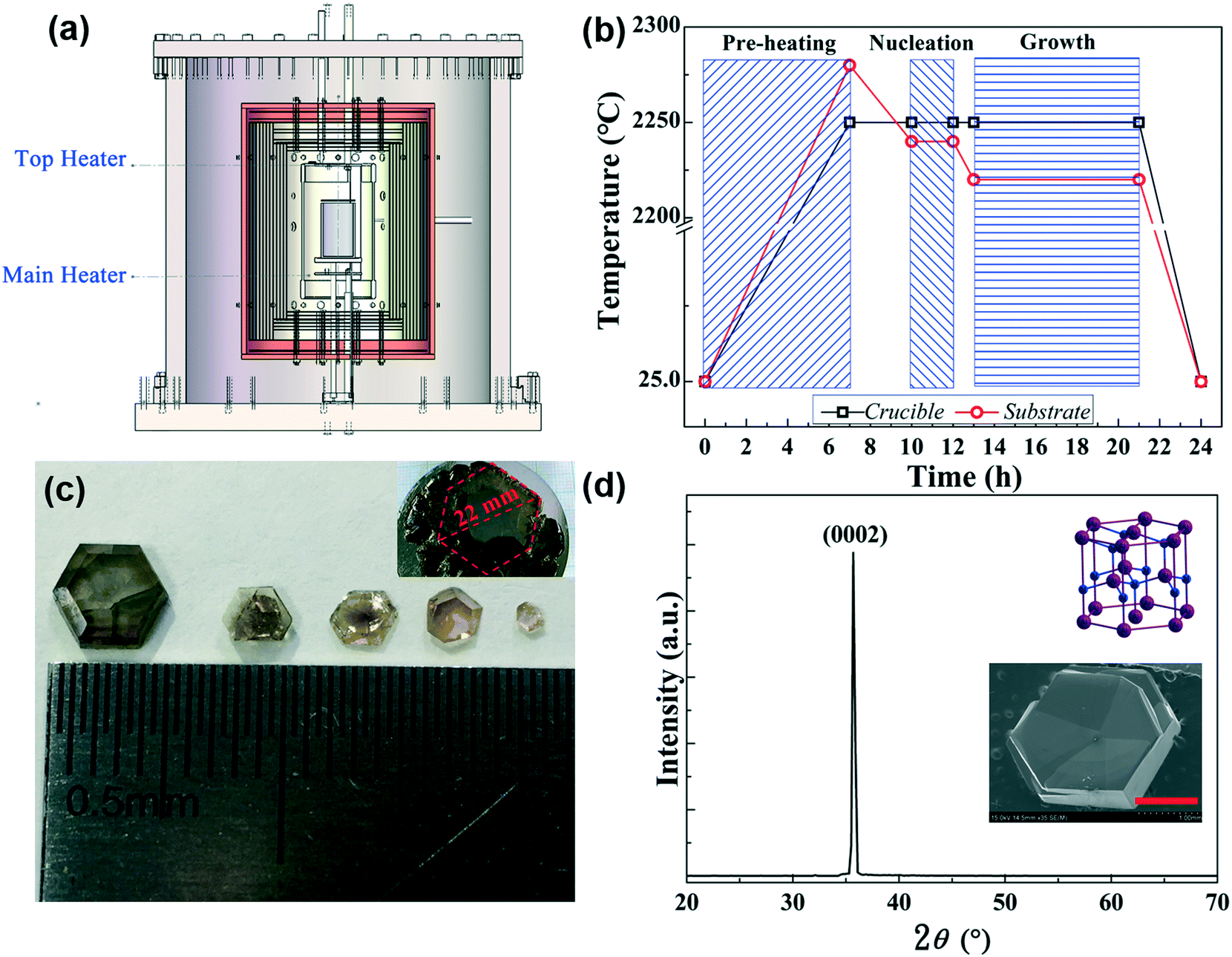 | ||
| Fig. 1 (a) Schematic of the configuration of the customized th-PVT furnace. (b) Temperature variation trends of the crucible and the substrate during the growth process of AlN BSCs. The line with square dots represents the temperature of the crucible. The line with circle dots represents the temperature of the substrate. Patterned areas represent different growth stages as indicated. (c) Image of the freestanding AlN bulk single crystals with different sizes. The inset shows the image of the largest AlN bulk single crystal with a diameter of about 22 mm. (d) X-ray diffraction pattern of an AlN crystal. The upper inset is the lattice structure of wurtzite AlN. The lower inset is the low magnification scanning electron microscopy image of a typical AlN crystal with a hexagonal facade, with a scale bar of 1 mm. | ||
Thereafter, temperature-dependent CL measurement on the AlN BSCs was carried out. The temperature was continuously increased from 8 K to 300 K. Fig. 2(a) shows the CL spectra in the deep-UV region. From the spectrum obtained at 8 K, a dominant peak at 206 nm (6.02 eV) with a shoulder at 208 nm (5.96 eV) can be resolved on a logarithm scale. The dominant peak can be clearly seen under all temperature conditions, and the shoulder diminishes with the increase of temperature. They both show red-shift with the increasing temperature. It is well known the valence band of wurtzite AlN near the Γ point splits into three bands: Γ7vbm (A), Γ9v (B), and Γ7v (C), in terms of transition energy increasing.26–30 Considering its consistent existence, the dominant emission at 206 nm can be assigned to a free A-exciton (FX) transition. The shoulder at 208 nm, which is 57 meV lower than the dominant line, can be identified as a donor bound exciton (I2) transition.27,29–31 The intensity of the I2 transition decreases with the increasing temperature because the donor bound excitons dissociate at high temperatures.27 The decrease of FX transition intensity with the increase of temperature can be attributed to the increase in nonradiative recombination.28 It has been reported that the temperature dependence of band edge free exciton energy in AlN is well-described by an equation:30
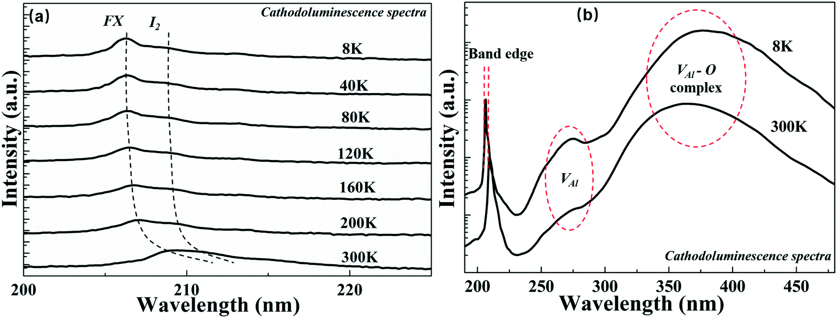 | ||
| Fig. 2 (a) Temperature-dependent cathodoluminescence spectra of AlN bulk single crystals in deep-UV region. (b) Cryogenic and room temperature cathodoluminescence spectra of AlN bulk single crystals in UV and visible regions. | ||
The free exciton energy E(T) decreases with the increasing temperature; this is consistent with the red-shift of the emissions shown in Fig. 2(a). It is noticed that the B- and C-exciton transition emissions are not distinguishable in the spectra perhaps because of the high fraction of FX transition.29 To gain more insight into the crystallinity of the AlN BSCs, the CL spectra at 8 K and 300 K were obtained in the visible region and are shown in Fig. 2(b). Besides near band edge emissions analyzed above, two extra emissions at longer wavelengths covering broad range were found in both spectra. Their peak positions at about 4.60 eV and 3.30 eV can be attributed to defect related luminescence of VAl and VAl–O complex, respectively.26,31 Especially, the broad coverages of the emission bands imply that more defect related energy states, such as VAl-shallow donor, are involved.31
Furthermore, X-ray photoelectron spectroscopy (XPS) was used to probe the elemental composition in AlN BSCs. The XPS patterns were demonstrated in Fig. 3(a). It clearly shows that besides Al and N elements, an appreciable O element exists in the crystals, which should be responsible for the defects of ON. Additionally, the atomic ratio of Al and N elements is supposed to be 1 in a perfect AlN crystal. Quantitative analysis of the XPS data revealed an atomic amount shortage of 7.3% for the Al element. This implies the existence of defects of VAl, which is consistent with the abovementioned CL emission result in near-UV-visible region. Moreover, the defect-related CL spectrum at 8 K was deconvoluted into five emission lines using partial Gaussian functions, as shown in Fig. 3(b). According to the literature,26,31 every line can be assigned to a specific defect-related energy transition, as shown in Table 1. It is noticed that in Fig. 2(b), the CL spectrum in the visible region shifts to higher energy in the temperature range from 8 K to 300 K. The reason can be speculated based on the deconvolution results. Emissions related to different defect states experience different influences from temperature. With the increase of temperature, the proportion of emissions related to CB–VAl/VAl–O complex transitions may become larger in the overall emissions; this induces a blue-shift of the whole spectrum. More studies are needed to address this issue.
 | ||
| Fig. 3 (a) X-ray photoelectron patterns of AlN BSCs showing the binding energies of Al 2p, Al 2s, N 1s and O 1s. (b) The CL spectrum of AlN BSCs at 8 K and the results of its deconvolution. | ||
| Line | Peak position (nm) | Energy (eV) | Attribution |
|---|---|---|---|
| A | 270 | 4.59 | CB → VAl3− |
| B | 340 | 3.65 | CB → (VAl–ON)2− |
| C | 366 | 3.39 | CB → (VAl–ON) |
| D | 393 | 3.16 | CB → (VAl–2ON) |
| E | 418 | 2.96 | VAl3−/2−/(VAl–2ON) → VB |
A device with the sandwich structure Au–AlN–W was fabricated by depositing a gold electrode on top of a crystal grown on a tungsten substrate. The device configuration is presented in the schematic illustration in the left inset in Fig. 4(a). Fig. 4(a) also shows the current–voltage (I–V) characterization with a bias applied to the W electrode. The nonlinear and asymmetric I–V curve indicates that both Au–AlN and W–AlN interfaces form non-ohmic contacts with different barriers.14,16,17,19,20,24 Among them, the W–AlN interface should be a Schottky contact considering that AlN has been grown directly on the W substrate. As for the Au–AlN side, either a Schottky barrier or a thin layer of Al2O3 grown on AlN surface is responsible for the parasitic resistance.24,32 Moreover, it was found that the Au–AlN–W device emitted white light under electrical bias, and the luminescence intensity increased with the increasing bias. The right inset in Fig. 4(a) shows that the device has a strong luminescence of white light under 60 V bias, and the spectrum is demonstrated in Fig. 4(b). Due to the limitation of the instruments, only defect-related luminescence in 250–1000 nm range was measured. The emission covers a wide range, indicating an abundant existence of deep and shallow energy states in the band gap.26 Additionally, PL measurements with an excitation laser of 177.5 nm and 405 nm at room temperature were carried out on the AlN crystal. Fig. 4(b) demonstrates the PL spectra and the EL spectrum in the same frame for comparison. These two PL spectra cover different wavelength regions, but both are included in the EL. It is well-known that luminescence originates from the recombination of carriers or the relaxation of excitons at these defect-related energy states, conduction band, and valence bands. Excitons generated by 177.5 nm lasers are at the highest energy state. Their relaxation emits light covering the band edge and all defect-related state emissions with more short wavelength composition. In contrast, under excitation at 405 nm, only excitons at defect-related low energy states can be generated. Their relaxation emits light with a long wavelength. This is consistent with previous reports.12,33 On the other hand, a high voltage bias can inject sufficient carries for all energy states and thus lead to all possible emissions.
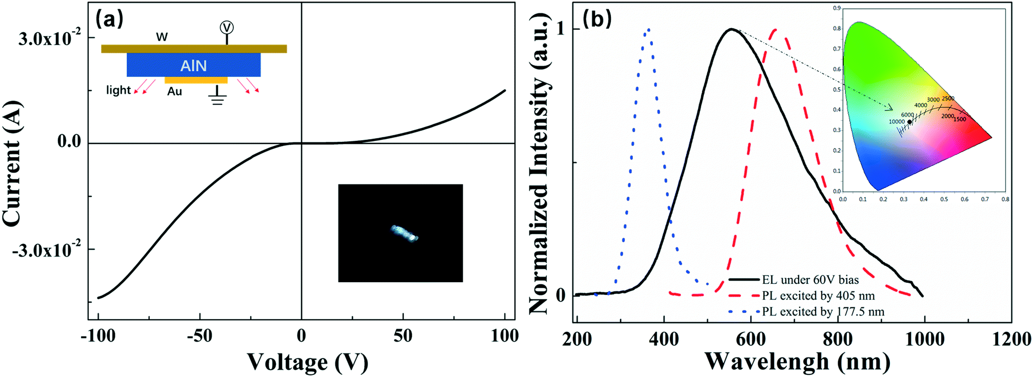 | ||
| Fig. 4 (a) Current–voltage curve of the Au–AlN–W device. The left inset shows the schematic of the sandwich device structure. The right inset shows the image of EL under 60 V bias. (b) The EL spectrum under 60 V bias (solid line), PL spectra excited by 405 nm (dash line) and 177.5 nm (dot line) of AlN crystals. The inset shows the color coordinates of the EL spectrum in CIE 1931 chromaticity diagram. | ||
Even though the defect-related luminescence is not favorable for the application of AlN crystals in the deep-UV field, it is worthy to note that the EL herein has a very high color quality. The color coordinate of the EL spectrum in 1931 CIE chromaticity diagram was calculated to be (0.33, 0.34), as shown in the inset of Fig. 4(b). The coordinate locates at the black body line with the correlated color temperature (CCT) at about 6500 K. Moreover, its color rendering index (CRI) was calculated to be about 97, which is very high in the illumination field.34,35 Notice that the traditional white light sources are based on either the combination of three primary color LEDs or the blue LED-exciting fluorescent powder. Thus, compared to these two indirect white light luminescence methods, the AlN crystals with the abovementioned EL property provide an alternative solution to create compact and solid-state white light sources.13 This benefits from the wide band gap of AlN, which can accommodate plenty of energy states. An elaborate control on the defect and impurity energy states may provide more possibilities in the EL property.
Conclusions
Freestanding wurtzite AlN BSCs with the size of up to 22 mm were grown using the th-PVT method. Temperature-dependent CL characterization shows that the AlN crystal has a good near band edge emission at 6.02 eV, revealing its application potential in deep-UV optoelectronic devices. Further investigation through EL and PL measurements demonstrates that the crystallinity of the AlN crystal has yet to be satisfactory as the defect-related energy states exist across the band gap. On the other hand, the high color quality of the defect-related luminescence, which originates from the universal existence of energy states in the forbidden band, paves a new path towards compact and solid white light LED.Conflicts of interest
There are no conflicts of interest to declare.Acknowledgements
Z. H. S. acknowledges the financial support received from the National Natural Science Foundation of China (grant no. 61505108), the Natural Science Foundation of Guangdong Province (grant no. 2016A030310055), and the Science and Technology Innovation Commission of Shenzhen (grant no. JCYJ20150625103602228). H. L. W. acknowledges the financial support received from the National Natural Science Foundation of China (grant no. 11447029, 61440028, 61136001) and the Science & Technology Bureau of Shenzhen (grant no. 20160520174438578). The authors are grateful to Mr. Fuchun Jiang for his assistance in XRD measurement, Ms. Guiwen Xu for her assistance in SEM measurement, and Mr. Zhixian Zhuang for drawing the schematic. The authors also appreciate Ms. Yali Liu and Prof. Peng Jin in the Institute of Semiconductors, Chinese Academy of Science, for their facility and help in CL and PL measurements.Notes and references
- H. Lu, W. J. Schaff, J. Hwang, H. Wu, G. Koley and L. F. Eastman, Appl. Phys. Lett., 2001, 79, 1489–1491 CrossRef CAS
.
- Y. X. Wu, J. J. Zhu, G. F. Chen, S. M. Zhang, D. S. Jiang, Z. S. Liu, D. G. Zhao, H. Wang, Y. T. Wang and H. Yang, Chin. Phys. B, 2010, 19, 036801 CrossRef
- H. Harima, T. Inoue, S. Nakashima, H. Okumura, Y. Ishida, S. Yoshida, T. Koizumi, H. Grille and F. Bechstedt, Appl. Phys. Lett., 1999, 74, 191–193 CrossRef CAS
- Z. G. Herro, D. Zhuang, R. Schlesser and Z. Sitar, J. Cryst. Growth, 2010, 312, 2519–2521 CrossRef CAS
- Y. B. Tang, H. T. Cong and H. M. Cheng, Appl. Phys. Lett., 2006, 89, 093113 CrossRef
- Q. Zhao, J. Xu, X. Y. Xu, Z. Wang and D. P. Yu, Appl. Phys. Lett., 2004, 85, 5331–5333 CrossRef CAS
- A. P. Huang, P. K. Chu and X. L. Wu, Appl. Phys. Lett., 2006, 88, 251103 CrossRef
- K. Tsubouchi and N. Mikoshiba, IEEE Trans. Sonics Ultrason., 1985, 32, 634–644 CrossRef
- E. Monroy, F. Omnes and F. Calle, Semicond. Sci. Technol., 2003, 18, R33–R51 CrossRef CAS
- F. A. Ponce and D. P. Bour, Nature, 1997, 386, 351–359 CrossRef CAS
- Y. Taniyasu, M. Kasu and T. Makimoto, Nature, 2006, 441, 325–328 CrossRef CAS PubMed
- S. Zhao, A. T. Connie, M. H. T. Dastjerdi, X. H. Kong, Q. Wang, M. Djavid, S. Sadaf, X. D. Liu, I. Shih, H. Guo and Z. Mi, Sci Rep, 2015, 5, 8332 CrossRef CAS PubMed
- E. F. Schubert and J. K. Kim, Science, 2005, 308, 1274–1278 CrossRef CAS PubMed
- W. Zheng, F. Huang, R. S. Zheng and H. L. Wu, Adv. Mater., 2015, 27, 3921–3927 CrossRef CAS PubMed
- H. M. Huang, R. S. Chen, H. Y. Chen, T. W. Liu, C. C. Kuo, C. P. Chen, H. C. Hsu, L. C. Chen, K. H. Chen and Y. J. Yang, Appl. Phys. Lett., 2010, 96, 062104 CrossRef
- S. Nikishin, B. Borisov, M. Pandikunta, R. Dahal, J. Y. Lin, H. X. Jiang, H. Harris and M. Holtz, Appl. Phys. Lett., 2009, 95, 054101 CrossRef
- A. BenMoussa, J. F. Hochedez, R. Dahal, J. Li, J. Y. Lin, H. X. Jiang, A. Soltani, J. C. De Jaeger, U. Kroth and M. Richter, Appl. Phys. Lett., 2008, 92, 022108 CrossRef
- J. Li, Z. Y. Fan, R. Dahal, M. L. Nakarmi, J. Y. Lin and H. X. Jiang, Appl. Phys. Lett., 2006, 89, 213510 CrossRef
- R. Dahal, T. M. Al Tahtamouni, Z. Y. Fan, J. Y. Lin and H. X. Jiang, Appl. Phys. Lett., 2007, 90, 263505 CrossRef
- R. Dahal, T. M. Al Tahtamouni, J.
Y. Lin and H. X. Jiang, Appl. Phys. Lett., 2007, 91, 243503 CrossRef
- S. B. Schujman, L. J. Schowalter, R. T. Bondokov, K. E. Morgan, W. Liu, J. A. Smart and T. Bettles, J. Cryst. Growth, 2008, 310, 887–890 CrossRef CAS
- R. T. Bondokov, S. G. Mueller, K. E. Morgan, G. A. Slack, S. Schujman, M. C. Wood, J. A. Smart and L. J. Schowalter, J. Cryst. Growth, 2008, 310, 4020–4026 CrossRef CAS
- D. Zhuang, Z. G. Herro, R. Schlesser and Z. Sitar, J. Cryst. Growth, 2006, 287, 372–375 CrossRef CAS
- H. Wu, R. Zheng, Y. Guo and Z. Yan, Mater. Res. Innovations, 2015, 19, 1153–1155 Search PubMed
- S. G. Mueller, R. T. Bondokov, K. E. Morgan, G. A. Slack, S. B. Schujman, J. Grandusky, J. A. Smart and L. J. Schowalter, Phys. Status Solidi A, 2009, 206, 1153–1159 CrossRef CAS
- T. Koppe, H. Hofsass and U. Vetter, J. Lumin., 2016, 178, 267–281 CrossRef CAS
- J. Li, K. B. Nam, M. L. Nakarmi, J. Y. Lin, H. X. Jiang, P. Carrier and S. H. Wei, Appl. Phys. Lett., 2003, 83, 5163–5165 CrossRef CAS
- Y. Taniyasu and M. Kasu, Appl. Phys. Lett., 2011, 98, 131910 CrossRef
- K. Y. Li, W. Y. Wang, Z. H. Chen, N. Gao, W. H. Yang, W. Li, H. Y. Chen, S. P. Li, H. Li, P. Jin and J. Y. Kang, Sci Rep, 2013, 3, 3551 CrossRef PubMed
- M. Feneberg, R. A. R. Leute, B. Neuschl, K. Thonke and M. Bickermann, Phys. Rev. B: Condens. Matter Mater. Phys., 2010, 82, 075208 CrossRef
- T. Onuma, T. Shibata, K. Kosaka, K. Asai, S. Sumiya, M. Tanaka, T. Sota, A. Uedono and S. F. Chichibu, J. Appl. Phys., 2009, 105, 023529 CrossRef
- A. Mahmood, R. Machorro, S. Muhl, J. Heiras, F. F. Castillon, M. H. Farias and E. Andrade, Diamond Relat. Mater., 2003, 12, 1315–1321 CrossRef CAS
- S. H. Shah, G. Nabi, W. S. Khan, A. Majid, C. B. Cao, S. Ali, M. Hussain, A. Nabi, S. Ishaq and F. K. Butt, Mater. Lett., 2013, 107, 255–258 CrossRef
- S. Nizamoglu, G. Zengin and H. V. Demir, Appl. Phys. Lett., 2008, 92, 031102 CrossRef
- J. H. Oh, S. J. Yang, Y. G. Sung and Y. R. Do, Opt. Express, 2012, 20, 20276–20285 CrossRef PubMed
| This journal is © The Royal Society of Chemistry 2017 |