
GeTe: a simple compound blessed with a plethora of properties
Jos E.
Boschker
 ,
Ruining
Wang
and
Raffaella
Calarco
*
,
Ruining
Wang
and
Raffaella
Calarco
*
Paul-Drude-Institut für Festkörperelektronik, Hausvogteiplatz 5-7, 10117 Berlin, Germany. E-mail: calarco@pdi-berlin.de
First published on 17th August 2017
Abstract
GeTe is a rather unconventional and complex compound from a fundamental point of view considering its very simple stoichiometry. Within this review, we first discuss the crystal structure of GeTe, focusing our attention on the bonding mechanism and on the distortion of the unit cell. This distortion is responsible for the ferroelectric properties of GeTe that are also considered here. Furthermore, we describe the amorphous phase and review the phase change material properties resorting to examples from several GeTe based alloys. Finally we examine the usage of GeTe for spintronics, a fairly recent application field.
 Jos E. Boschker | Jos E. Boschker received his BSc and MSc degrees from the University of Twente, the Netherlands. In 2012, he obtained his PhD from the Norwegian University of Science and Technology. After 4 years of post-doctoral work at the Paul-Drude-Institute für Festkörperelektronikk, he joined the Leibniz Institute for crystal growth, both in Berlin, Germany. His research interests include, among others, phase change materials, 2D materials, oxides and epitaxial thin film growth. |
 Rui Ning Wang | Rui Ning Wang freshly received his Ph.D. in Physics from the University of Humboldt for his work at the Paul-Drude-Institut in Berlin. His previous masters studies in Materials Science at the EPFL in Lausanne were targeted at semiconductor materials for microelectronics, a specialization that he further pursued with his latest work on epitaxial growth and characterization of GeTe and chalcogenide superlattices for electrical memory applications. |
 Raffaella Calarco | Raffaella Calarco received her MSc degree in Physics in 1996 from the University of Rome Tor Vergata in Italy and her Ph.D. in Materials Science in 2001 from the University of Rome La Sapienza, Italy. After one year of post-doctoral work at the RWTH Aachen University, Germany, she was with the Research Center Jülich, Germany. In 2010, she received the Habilitation in Physics from the RWTH Aachen and in 2012 from the Humboldt University in Berlin, Germany. Since 2010, she has been a Senior Scientist at the Paul-Drude-Institut in Berlin Germany. Her current research interests include epitaxy of phase-change materials and III-nitrides. |
Introduction and motivation
Since the middle of the past century, germanium telluride (GeTe) has been investigated both from a fundamental and technological perspective; constant progress has been implemented in the thermoelectric,1,2 ferroelectric,3–5 and phase-change material fields.6–8 In addition, GeTe recently entered the spintronic field when the giant bulk Rashba spin splitting in GeTe was first predicted9 and later experimentally demonstrated.10,11Such an abundant bundle of functionalities in GeTe is fairly surprising, looking at its very simple stoichiometry and the two-atom rhombohedral unit cell that is commonly used to describe it. This is the case because the complexity of the material is more subtly residing in the interplay between the 10% of intrinsic Ge vacancies in the Ge sublattice,12 the rhombohedral distortion caused by the electronic Peierls instability of the rock-salt structure,13 and its 6-fold coordinated resonant bonding, which is a violation of the octet rule.14
Nowadays in the literature, the three phenomena mentioned above are invoked as responsible for many properties of GeTe. More specifically, the crystalline/amorphous switching mechanism has been attributed to the formation and disordering of a 6-fold resonant bonded network,15,16 while the rhombohedral distortion and spontaneous electric polarization of α-GeTe have been ascribed to an ordered Peierls dimerization.17 The large number of intrinsic Ge vacancies has been shown to be responsible for the p-type metallic conduction.18,19 In its amorphous phase (a-GeTe), it is covalently bonded, mainly in 4-fold coordinated sp3 tetrahedra,20 a configuration quite commonly found in amorphous semiconductors.21 In fact, the electrical and optical properties of a-GeTe are what one could expect from any amorphous semiconductor. It is really the crystalline phase of GeTe (c-GeTe) that displays extraordinary properties.
This review is organized as follows. First we discuss the crystal structure of GeTe and particular emphasis is given to the presentation of resonant bonding, Peierls distortion and Ge vacancies. Afterwards we briefly touch upon the amorphous phase and then consider the band structure of both phases. Finally we examine effects due to the combination of the three physical phenomena mentioned above, especially focusing on phase change, ferroelectric and magnetic doping properties. Thermoelectric and superconductive properties will not be discussed at length in this review.
Crystalline phase
To fully describe the GeTe crystalline structure, it is best to start with a simplified model, shown in Fig. 1a) where all Ge and Te atoms are sitting on their own sub-lattice, in a rock-salt structure. Incidentally, this cubic GeTe crystalline phase does exist at high temperature and is called the β-GeTe phase. The rock-salt structure is compatible with the necessity to accommodate six direct neighbors and is usually found for crystals with a stronger ionic character. However, the octahedral configuration in GeTe is stabilized by another phenomenon; it is due to resonant bonding.14–16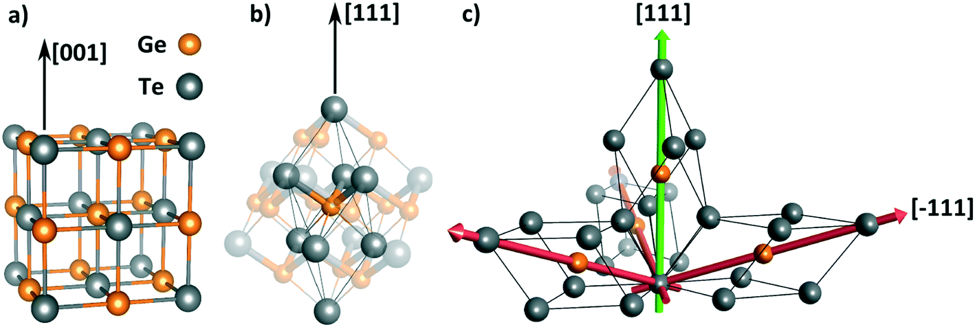 | ||
| Fig. 1 Schematic model of a) a cubic β-GeTe crystal with its rock-salt structure, b) α-GeTe, with the primitive cell in the rhombohedral coordinate system highlighted. The additional atoms of the distorted rock-salt unit cell are shown in a transparent overlay. c) A scale model of a α-GeTe crystal distorted along the [111] direction (green), with the three other possible directions of distortion along 〈−111〉 (red) (the directions are given for a cubic crystal system, while the cells represented are rhombohedral for visual clarity). | ||
The β-GeTe phase only exists above 630 K. The phase diagram of the Ge–Te system shows two stable low temperature phases.22 For a 50![[thin space (1/6-em)]](https://www.rsc.org/images/entities/char_2009.gif) :50 composition, the rhombohedrally distorted α-GeTe phase, i.e.Fig. 1c), is stable, whereas for Te contents above 51.2%, the orthorhombic γ-GeTe phase is stable. Interestingly, GeTe crystals with Te contents in the range of 50.6–51.2% can be formed in the α and γ phases depending on the annealing conditions.22 Furthermore, upon application of pressure, α-GeTe first transforms into the cubic phase and subsequently to the orthorhombic phase at higher pressures.23 The latter is accompanied with an increase in the electrical resistance.23
:50 composition, the rhombohedrally distorted α-GeTe phase, i.e.Fig. 1c), is stable, whereas for Te contents above 51.2%, the orthorhombic γ-GeTe phase is stable. Interestingly, GeTe crystals with Te contents in the range of 50.6–51.2% can be formed in the α and γ phases depending on the annealing conditions.22 Furthermore, upon application of pressure, α-GeTe first transforms into the cubic phase and subsequently to the orthorhombic phase at higher pressures.23 The latter is accompanied with an increase in the electrical resistance.23
Resonant bonding
Both Ge and Te use electrons in their outer p shell to create bonds. Between them, they possess three electrons on average per atom. This amount is clearly insufficient for the formation of saturated bonds with all six neighbors. Instead, a compromise is reached by adopting a resonant state, as suggested already in 1973,24 stemming from the superposition of equivalent virtual states that form saturated bonds with only half of the neighbors. Bonding is therefore achieved in each of the three dimensions by one unsaturated resonant orbital, binding each atom with the two neighbors at opposite sides.14,25 This peculiar bonding mechanism that can neither be defined as ionic, nor as hybridized,19 is truly the origin of the distinct optical properties of c-GeTe such as high optical dielectric constants and high electronic polarizability. In fact, the p electron density is highly delocalized and polarizable, which has a critical incidence on the dielectric function and reflectivity of the material.14,26 Waghmare et al.27 analyzed the influence of the lone pair electrons on the bonding properties of IV–V compounds and concluded that the lone pair is the driving force for the structural distortions of these compounds. In addition, they attributed the anomalously large Born effective charges and the large dielectric constants of these materials to the competition between the tendency to form a metallic state and the opening of a bandgap due to a structural distortion.The lack of long range order in amorphous GeTe results in the absence of resonant bonding in the amorphous state and the presence of a distinct difference between the crystalline and amorphous phases.24 X-ray photoemission data showed that the valence band densities of states in amorphous and crystalline GeTe are very similar even though the bonding is very different.28 Later it was realized that the difference in optical properties between the two states is actually caused by a difference in the optical matrix elements.29,30 Specifically, the optical matrix elements are enhanced in the crystalline phase due the alignment of resonantly bonded p-orbitals.30
Unfortunately, it is difficult to predict if a material is resonantly bonded or not. At present, only first-principles calculations or experimental measurements of the dielectric constant can give an answer. As a rule of thumb, resonant bonding is favored in materials with low tendency to hybridization and low ionicity.17 In fact, a large hybridization leads to larger bond distortions whereas increasing ionicity diminishes the high charge delocalization.17 In general, the secret for the good stability of these bonds is to maintain an important overlap of the p orbitals. These bonds are less rigid in their orientation and length compared to hybridized bonds. In a purely intuitive approach, one can already conceive how this malleable and compliant crystal structure contributes to the phase-change properties of the material.
A fundamental question that is concerned with the ultimate limit for viability of resonant bonding might thus be raised. Purely from a logical perspective, the resonant bonds at the surfaces or interfaces are going to be defective compared to the bonds within the resonantly bonded network. In extremely thin films, the influence of the interface and surface is the greatest and the volume could be too small for the resonant bonds to be fully expressed. GeTe would then first arrange into an amorphous configuration until a certain volume is reached and resonant bonding becomes viable. Such a highly unconventional growth scenario was reported upon deposition of GeTe films on a hydrogen passivated Si(111) surface.31 Initially, for growth parameters that should yield a crystalline material, an amorphous film forms, as shown by reflection high-energy diffraction measurements (RHEED). Afterwards, at a critical thickness of 4 GeTe bilayers, the entire amorphous film crystallizes. This experimental scenario was supported by density functional theory calculations showing that ultrathin GeTe films do not utilize resonant bonding in contrast to the bulk phase. The ability of GeTe to first accumulate in its amorphous form and only later crystallize to find its epitaxial relationship could be used to engineer novel heterostructures based on similar phase change materials, expanding the breadth of possible combinations between substrates and epilayers otherwise limited by the rules of classic epitaxy. In classic epitaxy, the film is first forced to grow pseudomorphically. The accumulated strain is released through the formation of undesirable defects and dislocations once a certain critical thickness (hc) is reached (Fig. 2). In contrast, by “resonant bonding epitaxy”, an amorphous layer could be first deposited, preferably on an inert surface (Fig. 2). After a certain thickness is reached, the film would create a resonantly bonded network, undergoing solid phase epitaxy. Because a certain volume of the material is already accumulated, the epitaxial relationship is not entirely dominated by the interfacial energy anymore and a different epitaxial compromise could then be found. In this way potential defects in the film can be reduced.
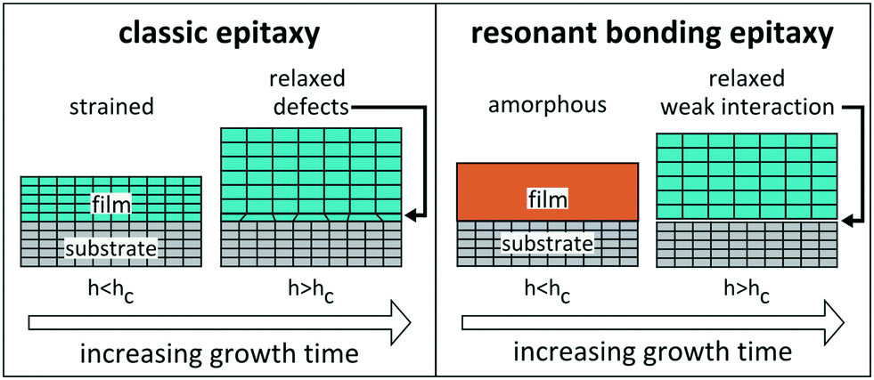 | ||
| Fig. 2 Schematic representation of the difference in the evolution of the films with increasing thickness for classical epitaxy and resonant bonding epitaxy. By the latter, the films grow first as amorphous and subsequently crystallizes. Since the crystalline phase is fully relaxed upon formation, this ensures a particularly low number of growth defects. | ||
Peierls distortion
The best proof of the compliance in this resonant structure resides in the second fundamental phenomenon that defines its shape: Peierls distortions, also called the Jahn–Teller effect, when applied to covalent molecules. These terms describe the intrinsic desire for any metallic periodic chain of atoms (with partially filled atomic orbitals) to form dimers because from an electronic point of view, going from a mono-atomic chain to di-atomic means splitting the single metallic band into two separate bands and opening a bandgap at the Fermi level. This has the effect of stabilizing the system by lowering slightly the energy of the occupied states, while raising the level of the empty conduction band. Of course, the trade-off is that the elastic energy is increased because the atoms are displaced from their ideal positions.13 This is illustrated schematically in Fig. 3. Please note that the scheme presents a half-filled band. In principle, any degree of partial band filling has an associated charge density wave distortion and is thus capable of Peierls distortion. | ||
| Fig. 3 Schematic band diagrams showing the electronic stability gained by dimerization of a mono-atomic chain. | ||
The displacement of atoms does not cost so much elastic energy in resonantly bonded structures because of their compliance and high electron delocalization as discussed above. As long as the p orbitals overlap each other, the structure maintains a good stability.18 In GeTe, the Peierls distortion results in the formation of alternated short strong bonds and longer weaker ones.14,32 Incidentally, it has been shown to be favorable for these short and long bonds to be distributed in an orderly fashion, into layers in the [111] direction.33 As a result, the crystal is elongated in this direction, leading to a rhombohedral distortion of the cubic rock-salt unit cell. The structure of α-GeTe found at room temperature (RT) is thus obtained, as illustrated in Fig. 1b). In this schematic model, the short strong bonds are represented by thicker connectors, while the long weak bonds are thinner.
The direct consequence of this ordered rhombohedral distortion is a shift of the Ge sublattice with respect to the Te atoms. The two sublattices no longer share the same center of charge; a ferroelectric polarization is induced in α-GeTe.3,5,34,35 At a longer range, this dipolar moment also exists spontaneously, already without prior polarization by an external field. The favorable ordering of the Peierls distorted bonds acts like a driving force, guiding and aligning the polarization direction in neighboring crystalline unit cells. A scale model is shown in Fig. 1c) to illustrate how the different directions of distortion and how the domains would fit with each other. A different axis of rhombohedral distortion also implies that the ferroelectric polarization in these domains will follow this alternative direction.
As stated above, GeTe adopts a cubic β-GeTe structure at high temperature (720 K). Even though the structure of GeTe in its ferroelectric phase is well characterized, the transition to the non-ferroelectric cubic phase is not well understood. Neutron diffraction studies have shown that the displacement of the Ge atoms with respect the Te atoms is reduced when the temperature is increased and that the rhombohedral distortion is reduced simultaneously, see Fig. 4.36,37 Interestingly, a reduction of the unit cell volume was observed at the phase transition37 and Raman spectroscopy measurements revealed a softening of the phonons in GeTe with increasing temperature.38 Both measurements indicate that the transition is displacive of nature. Analysis of the strain that occurs at the phase transition indicates that the transition is a weak first order displacive phase transition and thus close to tricritical.39 The displacive picture is also in agreement with recent phonon calculations that showed that the rhombohedral phase is due to a condensation of three optical active phonons at the center of the Brillouin zone.40
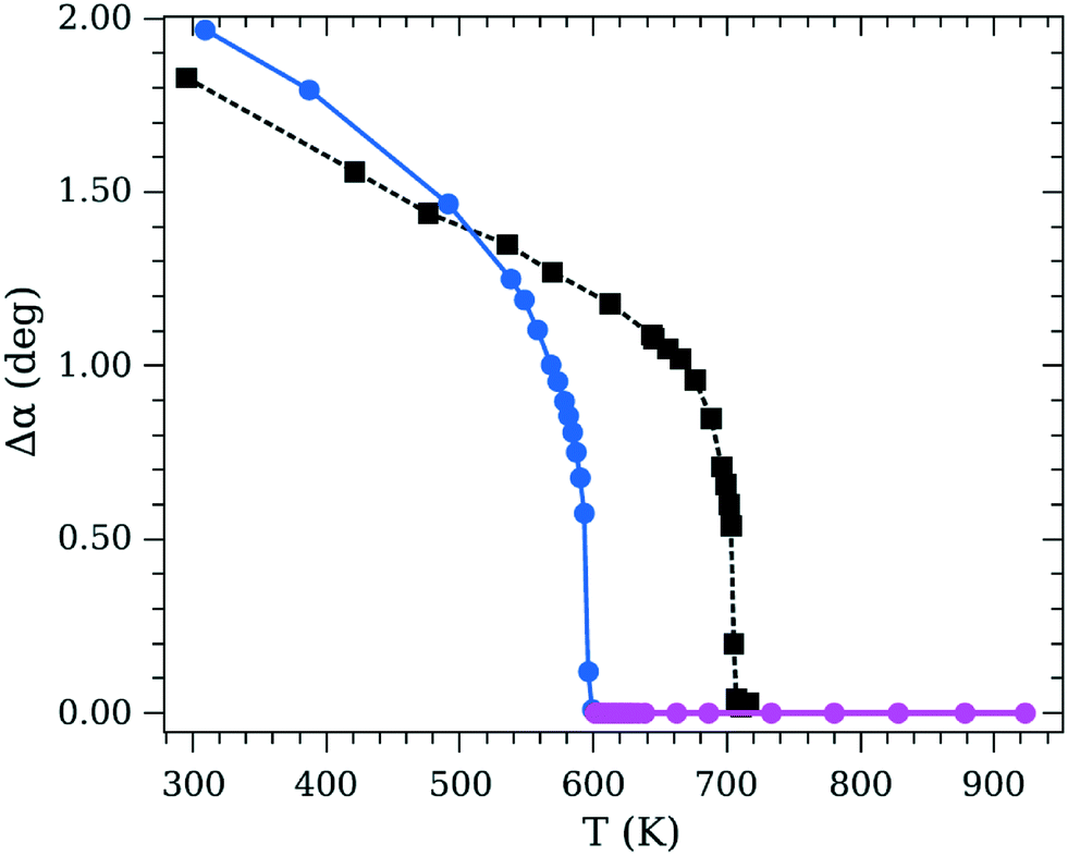 | ||
| Fig. 4 Rhombohedral distortion of GeTe as a function of temperature. Adapted with permission from ref. 37. Copyrighted by the American Physical Society. | ||
However, recently, the local chemical environments were probed using EXAFS41 and total scattering X-ray scattering combined with pair distribution analysis.42,43 These studies, see for example Fig. 5, showed that the length of the short and long Ge–Te bonds remains unchanged with temperature. Hence, it was concluded that the Peierls distortion is still present above the Curie temperature. Moreover, Hudspeth et al. determined that the correlation length of the Peierls distortions is approximately 20 Å in the cubic phase.43 This implies that GeTe is locally distorted above the Curie temperature, but not on average and thus that the transition from the high temperature phase to the low temperature phase should be driven by an ordering of the local distortions. Recent investigation on GeTe by means of resonant ultrasound spectroscopy indeed found a significant order/disorder contribution to the rhombohedral/cubic phase transition.39 The rhombohedral to cubic transition thus depends on an interplay of displacive components and disorder/order components. More detailed studies are clearly needed in order to complete our understanding of the phase transition of GeTe. In particular, the influence of the presence of Ge vacancies might be related to the observed spread in the transition temperatures40 and has not been addressed thoroughly, as it might be difficult to discriminate it from intrinsic contributions due to the first order transition.
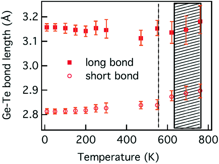 | ||
| Fig. 5 GeTe bond length as function of temperature. Reproduced from and adapted with permission from Fons et al.41 Copyrighted by the American Physical Society. | ||
The high conductivity of GeTe complicates the direct investigation of ferroelectric switching by conventional electrical techniques as the large amount of free charge carriers screens the applied electric field inhibiting polarization reversal. The investigation into the ferroelectric domain structure on the nanometer scale was first achieved by the usage of piezoresponse force microscopy (PFM).3 Later, the ferroelectric switching of epitaxial GeTe films was demonstrated using a resonance-enhanced PFM approach.5 This experiment was later on successfully reproduced.10
As seen before, ultra-thin epitaxial GeTe layers form first an amorphous film and subsequently crystallize,31 thus to understand the viability of Peierls distortions in a confined system, the same authors investigated the case of growth of GeTe on the  surface,44 where this amorphous transition is avoided, meaning that the interface containing Sb is able to stabilize the resonant bonds. RHEED was used to probe the earliest stage of the growth and during the deposition of the first two GeTe BLs, an in-plane lattice spacing larger than expected was measured (shown in Fig. 6). Raman measurements showed that for such thin layers, all modes are suppressed, which indicates that the crystal structure at this stage is not α-GeTe. This implies that the material does not possess its ferroelectric properties yet. Furthermore, DFT calculations exclude the cubic β-GeTe structure and support the Raman experimental data only using layers with in-plane lattice parameters fixed to the experimental value. The non-viability of Peierls distortions or the lack of their coherent ordering is thus identified as responsible for the formation of a different GeTe phase in such ultra-thin films.
 | ||
Fig. 6 {![[2 with combining macron]](https://www.rsc.org/images/entities/char_0032_0304.gif) 11} Lattice plane spacing during the first 200 seconds of GeTe growth. The in-plane spacing is larger with respect to α-GeTe. Figure adapted with permission from Macmillan Publishers Ltd: Sci. Rep. (ref. 37). © 2016. 11} Lattice plane spacing during the first 200 seconds of GeTe growth. The in-plane spacing is larger with respect to α-GeTe. Figure adapted with permission from Macmillan Publishers Ltd: Sci. Rep. (ref. 37). © 2016. | ||
Intrinsic Ge vacancies
GeTe displays p-type conduction and a carrier concentration of the order of 1020 cm−3 is typically measured.45–47 The reason for this behavior has been identified in the presence of defects in the form of Ge vacancies in a far from negligible concentration of 8–10% on the Ge sublattice.12 These defects have been shown to have the lowest formation energy among a collection of different possible candidates.19 In fact, starting from a perfect crystal, with a Fermi level in the middle of the bandgap, the formation energy of Ge vacancies is even negative, meaning that they will form spontaneously and are intrinsic to the material.In the same publication, it has been shown that the germanium vacancy is “self-healing”, meaning that upon removal of one Ge atom, the neighboring Te atoms keep their three-fold resonant p orbitals and simply bind more strongly to the other Ge atom still present on the other side. But these p states still need the electrons previously provided by the Ge atom. With the removal of each Ge atom, only the associated s state is truly removed, with its concomitant need for two electrons. But four outer-shell electrons are taken out of the system. Therefore, each vacancy leads to a total of two missing electrons, or in other words, the formation of two holes. In the band diagram, the introduction of these intrinsic holes will lead to a lowering of the Fermi level toward the valence band. And as the Fermi level is lowered, the formation energy of further vacancies gradually increases and becomes less likely. By the time an equilibrium concentration of Ge vacancies is reached, the Fermi level is already in the top part of the valence band, giving rise to GeTe its characteristics but at first unexpected p-type conduction. Combined with the intrinsic ferroelectric polarization, these two electric properties are not often found in the same material.
It is interesting to make here a quick estimation of the expected density of carriers from the concentration of vacancies: considering a rock-salt-like Ge4Te4 unit cell with a cell parameter of 6 Å, one cubic centimeter contains 4.6 × 1024 unit cells. Each cell contains four Ge sublattice sites, 8% of these sites contain vacancies, and each vacancy contributes two carriers. In theory, in a perfect crystal, the Ge vacancies should contribute to a carrier concentration of ∼3 × 1021 cm−3. This value is higher than the experimentally measured 1020 cm−3, but does not take into account all other possible defects that could trap or annihilate the carriers (grain boundaries, oxygen or silicon contamination). This simple estimate remains a good indication that all free carriers in GeTe probably originate from these vacancies.
Edwards et al.19 have calculated that vacancies should not play an important role in the crystalline structure of GeTe despite their important concentration, since the introduction of these defects only barely repositions the neighboring Te atoms. They could, however, play an important role in the phase switching mechanism, as it has been calculated that they provide convenient pathways for the diffusion of Ge atoms,48 helping in the necessary rearrangement of atoms between the two phases. Vacancies are also present in Ge–Sb–Te ternary compounds (GST), where they play an even more important role, as their ordering into layers has been shown to drive a metal–insulator transition or to grant topological insulator properties.49,50
Besides influencing the electrical conductivity, the large amount of Ge vacancies present in α-GeTe also influences the thermal and thermoelectric properties of α-GeTe. For example, Shaltaf et al.51 showed that the phonon dispersion of α-GeTe changes when a significant number of holes are added to the system. In particular, for a hole concentration of 2.1 × 1021 cm−1 the A1 longitudal optical phonon shifts from 153 cm−1 to 115 cm−1. Based on these calculations, Shaltaf et al. demonstrated that the specific heat also depends on the carrier concentration.51 Using a similar approach, it was also demonstrated that the lattice thermal conductivity of GeTe depends on the carrier concentration.52 It should be noted that the thermal conductivity is also strongly affected by doping GeTe with, for example, N.53 Finally, the Seebeck coefficient is strongly dependent on the carrier concentration and ranges from 180 to 25 μV K−1 for carrier concentrations between 3 × 10¹⁹ and 6 × 1020 cm−1.54 Importantly, the Seebeck coefficient of GeTe is significantly larger than the Seebeck coefficient of PbTe at a given carrier concentration.54 Due to the low electrical resistance, high power factors (up to 42 μW cm−1 K−2) can be achieved in GeTe, making GeTe one of the most promising material bases for thermoelectric applications.54
The rhombohedral α-GeTe phase shows an indirect band gap of 0.5 eV with the Fermi level inside the valence band.55 The band gap of the amorphous phase amounts instead to 0.8 eV.56 Between the two phases, 6 orders of magnitude of electrical contrast was measured (resistivity of the amorphous from 102–103 Ω cm and crystalline in the range of 4 × 10⁻⁴ Ω cm).56
Amorphous phase
The structure of the amorphous phase of GeTe has long been considered as completely random. Much information was derived also by studying GeTe alloyed with Sb to form GeSbTe (GST). It was found from the extended X-ray absorption fine structure (EXAFS) carried out on both as-deposited57,58 and laser-amorphized GST59 that in comparison to the crystalline structure, the Ge–Te and Sb–Te bonds are shorter. This is a very unusual feature as a simple randomization of a covalent crystal results usually in the elongation of the bond length. The amorphous phase can thus be considered to possess a higher local order. The EXAFS experiments on the laser amorphized material (or melt-quenched phase) indicated a local tetrahedral Ge coordination. Thus, the coordination change from octahedral in the crystalline to tetrahedral in the amorphous phase was named umbrella-flip.59 However, multiple coexisting local environments in the amorphous material were suggested after photo-electron spectroscopy on the core-levels of Ge 2p and Sb 3d that revealed only a very weak asymmetric shift.60Later on, first principles molecular dynamics simulations revealed the coexistence of tetrahedral and defective octahedral-like structures.61–65 From the total and partial pair correlation functions, the presence of homopolar Ge–Ge bonds was shown. These types of bonds are referred to as “wrong bonds” as they are absent in the crystalline phases.
Nevertheless four-membered ring (shown in Fig. 7) building blocks of the crystalline phase were found also in the amorphous phase,66,67 which thus partially retains the coordination typical of the crystalline structure. The absence of a medium-range order, however, impedes the formation of resonant bonds. This results in a lower reflectivity with respect to the crystal arising from the lower static polarizability of homopolar bonds.14
 | ||
| Fig. 7 Molecular dynamics calculation of rapidly quenched amorphous GST showing high concentrations of crystal seeds in the form of connected four-membered rings. Figure adapted with permission from Macmillan Publishers Ltd: Nature (ref. 50). © 2008. | ||
The phase change archetype
Phase change materials represent a class of materials that can be switched reversibly between at least an amorphous and a crystalline phase. Due to the differences in the bonding nature and atomic arrangement, a striking change in the optical and electrical properties occurs between the amorphous phase with low reflectivity and high resistance and the crystalline phase with high reflectivity and low resistance.14,29,56,68 The latter, being the more stable phase, can be obtained from the amorphous phase by bringing the material to the crystallization temperature (Tx) and giving it enough time to let the structure reorganize (see Fig. 8). On the other hand, a strong spike in energy that sends the material above the melting point (Tm) can disorganize the crystalline phase; the material can then be frozen in its metastable amorphous phase by a rapid quenching. For technological purposes, the amorphization is often called the power limiting process because of the energy needed to reach Tm, while crystallization is data rate limiting because of the time needed to let crystallization take place.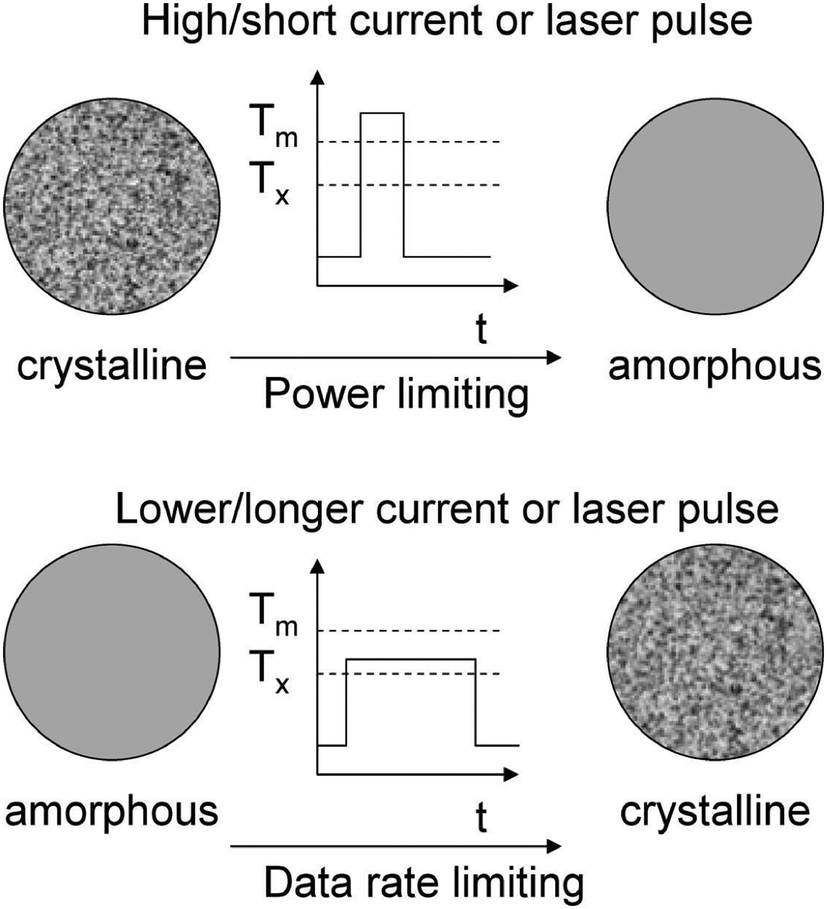 | ||
| Fig. 8 Schematic of the phase change processes as a function of time (t). Reprinted (adapted) with permission from ref. 68 (Raoux, S., Wełnic, W. & Ielmini, D. Phase change materials and their application to nonvolatile memories, Chem. Rev., 2010, 110, 240–267). Copyright (2010) The American Chemical Society. | ||
Switching between the two phases can be triggered on a very short timescale and at a reasonable energy cost,69 in a way that almost seems paradoxical, considering how contrasting their properties are. It is therefore no surprise that these materials have been exploited during the past two decades in optical data storage applications such as rewritable CDs, DVDs, and now blue-ray discs.70 More recently, efforts have also been invested to utilize more specifically the change in electrical properties of such materials in non-volatile electronic memory devices.68,70–76 In all these applications, the most commonly used materials as well as the most promising future candidates are chalcogenides.70 This term simply refers to the chemical compounds containing one or more elements from the sixth column of the periodic table (excluding oxygen).
Among different compounds exhibiting phase change properties, the most interesting are Te-based GST alloys, as they switch efficiently within nanoseconds between phases. GeTe is analogous to the more complex GST ternary alloys in terms of switching properties, but it is a binary material. Thus it was widely studied to understand the switching mechanism of GST alloys.
As discussed previously, the amorphous phase of GeTe is fairly similar to the local bonding geometry of the crystalline phase as it contains about 1/3 of the Ge atoms in a tetrahedral environment. The first atomistic model for the phase change mechanisms was proposed by A. V. Kolobov et al. (the umbrella-flip).59 An alternative mechanism of crystallization was actually proposed by Hegedüs and Elliott61 suggesting that the phase transition occurs thanks to a fast realignment of four-membered rings present in both the amorphous and crystalline phases.
However, one should consider that in PCM devices, crystallization occurs at a temperature above the glass transition temperature, at which the material is in a supercooled liquid state.77 Thus, this state dictates the properties for the high speed of crystallization typical for PCM. The fast crystallization was ascribed to the fragility of the liquid phase as demonstrated by ultra-fast differential scanning calorimetry measurements on GST78 and molecular dynamic simulations.79
Spintronic applications
At first sight one would not associate a ferroelectric material such as GeTe with spintronic applications that aim at manipulating the spin of electrons. Nevertheless, recent years have seen two interesting approaches that use GeTe exactly for this purpose. First, the alloying of GeTe with transition metal ions, such as Mn, Fe and Cr, is known to introduce ferromagnetism in GeTe (ref. 80, 81) and results in Curie temperatures (Tc) of approximately 190,82 160 (ref. 83) and 200 K,84 respectively. These GeTe alloys can thus be considered as a diluted semiconductor, similar to (Ga, Mn)As,85 but with additional advantage of a ferroelectric distortion. For brevity, we will only discuss the case of Ge1−xMnxTe, because it is the best studied example of alloying GeTe with a transition metal ion. The second approach relies on the giant and switchable Rashba spin splitting that is present in GeTe.9 These two approaches will be discussed below.Ferroelectric Rashba semiconductors
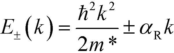
Rashba spin splitting is a well-known phenomenon in classical semiconductors.86,87 It is due to the inversion symmetry breaking that occurs for example at a (semiconductor) interface or surface. This results in an electric field perpendicular to the interface. Electrons that travel parallel to the interface experience this as an effective magnetic field, which lifts the spin degeneracy and splits the electronic bands into two bands with opposite spins:where ℏ is the reduced Planck constant, k is the momentum, m* is the effective electron mass and αR is the Rashba parameter. The Rashba parameter is proportional to the electric field induced by the breaking of the inversion symmetry and strength of the spin–orbit coupling (that depends on the atomic mass). For typical semiconductors, this effect is however rather small and αR = 0.07 eV Å for InGaAs/InAlAs semiconductor interfaces. In recent years, it was realized that the Rashba spin splitting is not limited to such systems, but occurs also in the bulk in rather special cases as for example in BiTeI for which a giant Rashba parameter of 3.8 eV Å was observed using angle resolved photoemission spectroscopy (ARPES).88 Di Sante et al.9 took this field a step further and predicted that GeTe has a giant bulk Rashba spin splitting (αR = 4.8 eV Å) that is due to the strong interplay between Rashba spin-splitting of electronic bands and ferroelectricity. The direction of the effective Rashba magnetic field in the semiconductor can thus be switched by simply reversing the dielectric polarization. Fig. 9 shows a zoom-in view of the band structure of GeTe around the Z-point as calculated by density functional theory with the PBE approximation. The splitting of the valence and conduction bands induced by the Rashba effect can clearly be recognized. The presence of a giant Rashba spin splitting in this material can be understood as the combination of four ingredients: atoms with a large spin–orbit interaction, lack of inversion symmetry, small band gap and the same symmetry character for the valence band maximum and the conduction band minimum. An electric field can be used to control the relative displacement of Ge with respect to Te or even switch it. Hence the term ferroelectric Rashba semiconductor was coined.89 Di Sante et al. envisioned that GeTe thus can be used in a Datta-Das type transistor9 and enable spin manipulation. The particular attractive feature of GeTe in this respect is the large Rashba parameter that makes it possible to flip the spin orientation within only 6 nm, which is much smaller than what is expected for conventional semiconductors.
 | ||
| Fig. 9 The electronic bands of α-GeTe around the Z-point as calculated by density functional theory in the PBE approximation. The splitting of the bands due to the Rashba effect can be observed. Adapted with permission from Di Sante et al.9 Copyright © 2013 Wiley-VCH Verlag GmbH & Co. KGaA, Weinheim. | ||
Since the prediction of a giant Rashba spin splitting, several groups have studied this effect using ARPES supported by band structure calculations.10,11,90,91 The observation of the bulk band structure of GeTe is however complicated by the presence of surface states and by the p-type character of GeTe. Initial ARPES measurements by Liebmann et al. revealed that these surface states also show a giant Rashba spin splitting of 0.14 Å−1 and found signatures of bulk Rashba bands.10 Furthermore, a direct connection between the ferroelectric polarization direction and Rashba effect was established.10 Subsequent investigations by two independent groups clearly established the presence of bulk Rashba bands in GeTe.11,90,91 Elmers et al. determined a spin splitting of 0.07 Å−1 of the bulk bands.11 Moreover, they found a two times higher spin polarization in the outer bulk Rashba bands indicating a complex hybridization of the bulk band. Krempaský et al. found an even larger spin splitting of 0.13 Å−1 and determined the Rashba parameter to be 4.2 eV Å.90 This is the highest known value for any material and in good agreement with the theoretical predictions.9 These properties make GeTe attractive for spintronic applications. The preliminary investigation indeed indicates that there is a spin to charge conversion in the GeTe/Fe heterostructure.92
(GeTe)1−x–(MnTe)x alloys
There are three different structural phases present in the bulk GeTe–MnTe phase diagram.93 Two are related to GeTe: the high temperature cubic NaCl structure and the low temperature rhomobohedral structure. The third phase is related to MnTe that crystallizes in the NiAs structure. Johnston et al. found that the NaCl and the NiAs structures exist together in compounds with an MnTe content of 0.5–0.9.93 MnTe can also be stabilized in a zinc-blende structure in thin films and the coexistence of NaCl and zinc blende structures has been observed for GeTe1−x–MnTex alloys with a MnTe content of 0.5 or above.94 It is worth pointing out that in general such effects of phase separation are not unusual for diluted magnetic semiconductors.Multiferroic applications require a material with both ferroelectric and magnetic polarizations. Fig. 10 shows the multiferroic phase diagram of GeTe1−x–MnTex. For GeTe1−x–MnTex alloys, it is observed that the rhombohedral distortions decrease with an increase in the Mn content. This results in a reduction of the critical temperature (Tc). The Curie temperature of the ferromagnetic phase increases reaching values of approximately 200 K for x = 0.5. Multiferroic properties are thus present in a wide range of compositions with a maximum Tc of around 100 K for the observation of multiferroic properties. It should be noted that the structural distortions are only observed up to x = 0.3 using X-ray diffraction measurements. The presence of structural distortions for a higher MnTe content is deduced from EXAFS measurements. The Peierls distortion in GeTe does not vanish in the high temperature cubic phase, so the presence of a Ge/Mn shift is not sufficient evidence to claim a ferroelectric phase. In conclusion, the observation of multiferroic effects up to 100 K for x = 0.5 indicates that ferroelectricity can be realized for this alloy.
 | ||
| Fig. 10 Multiferroic phase diagram of Mn-doped GeTe. Adapted with permission from Kriegner et al.95 Copyrighted by the American Physical Society. | ||
Curie temperatures of 190 K have been observed for GeMnTe alloys with a low Mn content (x = 0.08),82 in contrast with the phase diagram presented in Fig. 10 and measurements of bulk samples.81 Recently, Kriener et al. showed that the Curie temperature strongly depended on the cooling conditions for x < 0.1.96 When the samples were quenched from 900 K, a Curie temperature below 50 K was observed, whereas the cooling rate of 5 K h−1 resulted in higher Curie temperature with a maximum approximately 180 K, see Fig. 11. The difference between these two phases was attributed to phase separation into Mn rich and Mn poor regions. Moreover, they demonstrated the possibility of switching reversibly between the phases with a high and low Curie temperature by using appropriate cooling procedures, which adds another interesting functionality to the portfolio of GeTe.
 | ||
| Fig. 11 Curie temperature of Ge1−xMnxTe alloys that are slowly cooled and quenched from 900 K. Figure adapted with permission from Macmillan Publishers Ltd: Sci. Rep. (ref. 86), © 2016. | ||
The coupling of the ferroelectric and ferromagnetic order parameters was demonstrated by Przybylińska et al. in 2014.46 They used ferromagnetic resonance to probe the magneto crystalline anisotropy of GeMnTe alloys and found two different magneto crystalline anisotropies in samples with x = 0.2–0.5. It was argued that these two anisotropies correspond to domains with opposite ferroelectric polarizations. It should be noted that these two anisotropies where not observed for x < 0.2, which has a larger structural distortion than the x = 0.2–0.5 alloys. The presence of 〈−111〉 oriented domains besides the 〈111〉 orientation was not considered as a possible source of the observation of two crystalline anisotropies. Subsequently, the amount of domains with a given polarization was deduced from the intensities of the ferromagnetic resonance absorption. It was argued that the occupation changes upon the reversal of the magnetization and thus indicates a coupling between the ferroelectric and ferromagnetic properties.46 More studies on single phase GeMnTe samples are clearly needed in order to confirm these conclusions.
Finally, the coexistence of ferromagnetism and ferroelectricity results in a change of the electronic structure. As pointed out by Di Sante et al. and discussed above, bands with opposite spins in the ±kx,y direction split.9 The presence of ferromagnetism on the other hand lowers (increases) the energy of the band with spins pointing in the same (opposite) direction as the magnetization of the sample. In GeMnTe samples, both of these effects are present at the same time, as demonstrated by Krempaský et al.90 They observed an antiparallel alignment between the ferroelectric polarization and the magnetization and showed that the Rashba-type spin helicity is modified by switching the magnetization direction. In general, it can be concluded that the addition of ferromagnetism to ferroelectric semiconductors, such as GeTe, adds additional degrees of freedom for controlling the spin of electrons.
Outlook
Though a large amount of work was dedicated to investigate GeTe, there remains a lot of unsolved questions and areas of improvement in understanding. For instance, the investigation of ferroelectric properties of ultrathin GeTe layers should be extended and direct PFM investigations be performed. Furthermore, control of the intrinsic vacancy concentration and thus tuning of carrier concentration density by appropriate doping to allow the usage of GeTe in spintronic devices would be welcomed.Conflicts of interest
There are no conflicts to declare.Acknowledgements
This work was supported by the Leibniz Gemeinschaft within the Leibniz Competition on a project entitled: “Epitaxial phase change superlattices designed for investigation of non-thermal switching”. We would like to thank all the people that worked on PCM at PDI for their contribution to this field and Y. Takagaki for critical reading of the manuscript.References
- C. Wood, Materials for thermoelectric energy conversion, Rep. Prog. Phys., 1999, 51, 459–539 CrossRef
.
- D. Wu,
et al., Origin of the high performance in GeTe-based thermoelectric materials upon Bi2Te3 doping, J. Am. Chem. Soc., 2014, 136, 11412–11419 CrossRef CAS PubMed
- J. J. Gervacio-Arciniega, E. Prokhorov, F. J. Espinoza-Beltran and G. Trapaga, Characterization of local piezoelectric behavior of ferroelectric GeTe and Ge2Sb2Te5 thin films, J. Appl. Phys., 2012, 112, 52018 CrossRef
- M. J. Polking,
et al., Ferroelectric order in individual nanometre-scale crystals, Nat. Mater., 2012, 11, 700–709 CrossRef CAS PubMed
- A. V. Kolobov,
et al., Ferroelectric switching in epitaxial GeTe films, APL Mater., 2014, 2, 66101 CrossRef
- A. V. Kolobov,
et al., Why Phase-Change Media Are Fast and Stable: A New Approach to an Old Problem, Jpn. J. Appl. Phys., 2005, 44, 3345–3349 CrossRef CAS
- S. Raoux, H.-Y. Cheng, M. A. Caldwell and H.-S. P. Wong, Crystallization times of Ge–Te phase change materials as a function of composition, Appl. Phys. Lett., 2009, 95, 71910 CrossRef
- G. Bruns,
et al., Nanosecond switching in GeTe phase change memory cells, Appl. Phys. Lett., 2009, 95, 43108 CrossRef
- D. Di Sante, P. Barone, R. Bertacco and S. Picozzi, Electric control of the giant Rashba effect in bulk GeTe, Adv. Mater., 2013, 25, 509–513 CrossRef CAS PubMed
- M. Liebmann,
et al., Giant Rashba-Type Spin Splitting in Ferroelectric GeTe(111), Adv. Mater., 2016, 28, 560–565 CrossRef CAS PubMed
- H. J. Elmers,
et al., Spin mapping of surface and bulk Rashba states in ferroelectric α-GeTe(111) films, Phys. Rev. B, 2016, 94, 201403 CrossRef
- A. V. Kolobov, J. Tominaga, P. Fons and T. Uruga, Local structure of crystallized GeTe films, Appl. Phys. Lett., 2003, 82, 382 CrossRef CAS
- J.-P. Gaspard and A. Pellegatti, Marinelli, F. and Bichara, C. Peierls instabilities in covalent structures I. Electronic structure, cohesion and the Z = 8 - N rule, Philos. Mag. B, 1998, 77, 727–744 CrossRef CAS
- K. Shportko,
et al., Resonant bonding in crystalline phase-change materials, Nat. Mater., 2008, 7, 653–658 CrossRef CAS PubMed
- B. Huang and J. Robertson, Bonding origin of optical contrast in phase-change memory materials, Phys. Rev. B: Condens. Matter Mater. Phys., 2010, 81, 81204 CrossRef
- A. V. Kolobov, P. Fons, J. Tominaga and M. Hase, Excitation-Assisted Disordering of GeTe and Related Solids with Resonant Bonding, J. Phys. Chem. C, 2014, 118, 10248–10253 CAS
- D. Lencer,
et al., A map for phase-change materials, Nat. Mater., 2008, 7, 972–977 CrossRef CAS PubMed
- J. Lewis and E. Band, Structure and Nature of Lattice Defects in GeTe from Analysis of Electrical Properties, Phys. Status Solidi, 1969, 35, 737–745 CrossRef CAS
- A. Edwards,
et al., Electronic structure of intrinsic defects in crystalline germanium telluride, Phys. Rev. B: Condens. Matter Mater. Phys., 2006, 73, 45210 CrossRef
- M. Krbal,
et al., Selective detection of tetrahedral units in amorphous GeTe-based phase change alloys using Ge L3-edge x-ray appearance near-edge structure spectroscopy, Appl. Phys. Lett., 2013, 102, 111904 CrossRef
-
N. E. Mott and E. A. Davis, Electronic Processes in Non-Crystalline Materials, (Oxford Classic Texts in the Physical Sciences), Oxford University Press, 2012 Search PubMed
- D. I. Bletskan, Phase Equilibrium in the Systems AIV—BVI. Part 2. Systems Germanium—Chalcogen, J. Ovonic Res., 2005, 1, 53–60 Search PubMed
- A. Onodera, I. Sakamoto, Y. Fujii, N. Môri and S. Sugai, Structural and electrical properties of GeSe and GeTe at high pressure, Phys. Rev. B: Condens. Matter Mater. Phys., 1997, 56, 7935–7941 CrossRef CAS
- G. Lucovsky and R. M. White, Effect of resonance bonding on the properties of crystalline and amorphous semiconductors, Phys. Rev. B, 1973, 8, 660–667 CrossRef CAS
- D. Lencer, M. Salinga and M. Wuttig, Design rules for phase-change materials in data storage applications, Adv. Mater., 2011, 23, 2030–2058 CrossRef CAS PubMed
- P. B. Littlewood, The crystal structure of IV-VI compounds. I. Classification and description, J. Phys. C: Solid State Phys., 1980, 13, 4855 CrossRef CAS
- U. V. Waghmare, N. A. Spaldin, H. C. Kandpal and R. Seshadri, First-principles indicators of metallicity and cation off-centricity in the IV-VI rocksalt chalcogenides of divalent Ge, Sn, and Pb, Phys. Rev. B: Condens. Matter Mater. Phys., 2003, 67, 125111 CrossRef
- N. J. Shevchik, J. Tejeda, D. W. Langer and M. Cardona, Similarities in the Valence Bands of Amorphous and Crystalline GeTe Determined by X-Ray Photoemission, Phys. Rev. Lett., 1973, 30, 659 CrossRef CAS
- W. Wełnic, S. Botti, L. Reining and M. Wuttig, Origin of the Optical Contrast in Phase-Change Materials, Phys. Rev. Lett., 2007, 98, 236403 CrossRef PubMed
- B. Huang and J. Robertson, Bonding origin of optical contrast in phase-change memory materials, Phys. Rev. B: Condens. Matter Mater. Phys., 2010, 81, 81204 CrossRef
- R. Wang, W. Zhang, J. Momand, I. Ronneberger, J. E. Boschker, R. Mazzarello, B. J. Kooi, H. Riechert, M. Wuttig and R. Calarco, Formation of Resonant Bonding during Growth of Ultrathin GeTe Films, NPG Asia Mater., 2017, 9, e396 CrossRef CAS
- T. Nonaka, G. Ohbayashi, Y. Toriumi, Y. Mori and H. Hashimoto, Crystal structure of GeTe and Ge2Sb2Te5 meta-stable phase, Thin Solid Films, 2000, 370, 258–261 CrossRef CAS
- V. L. Deringer, M. Lumeij and R. Dronskowski, Ab Initio Modeling of α-GeTe(111) Surfaces, J. Phys. Chem. C, 2012, 116, 15801–15811 CAS
- F. Kadlec, C. Kadlec, P. Kužel and J. Petzelt, Study of the ferroelectric phase transition in germanium telluride using time-domain terahertz spectroscopy, Phys. Rev. B: Condens. Matter Mater. Phys., 2011, 84, 205209 CrossRef
- M. J. Polking,
et al., Size-Dependent Polar Ordering in Colloidal GeTe Nanocrystals, Nano Lett., 2011, 11, 1147–1152 CrossRef CAS PubMed
- T. Chattopadhyay, J. Boucherle and H. G. von Schnering, Neutron diffraction study on the structural phase transition in GeTe, J. Phys. C: Solid State Phys., 1987, 20, 1431 CrossRef CAS
- T. Chatterji, C. M. N. Kumar and U. D. Wdowik, Anomalous temperature-induced volume contraction in GeTe, Phys. Rev. B: Condens. Matter Mater. Phys., 2015, 91, 54110 CrossRef
- E. F. Steigmeier and G. Harbeke, Soft phonon mode and ferroelectricity in GeTe, Solid State Commun., 1970, 8, 1275–1279 CrossRef CAS
- D. Yang, T. Chatterji, J. A. Schiemer and M. A. Carpenter, Strain coupling, microstructure dynamics, and acoustic mode softening in germanium telluride, Phys. Rev. B, 2016, 93, 144109 CrossRef
- U. D. Wdowik, K. Parlinski, S. Rols and T. Chatterji, Soft-phonon mediated structural phase transition in GeTe, Phys. Rev. B: Condens. Matter Mater. Phys., 2014, 89, 224306 CrossRef
- P. Fons,
et al., Phase transition in crystalline GeTe: Pitfalls of averaging effects, Phys. Rev. B: Condens. Matter Mater. Phys., 2010, 82, 155209 CrossRef
- T. Matsunaga, P. Fons, A. V. Kolobov, J. Tominaga and N. Yamada, The order-disorder transition in GeTe: Views from different length-scales, Appl. Phys. Lett., 2011, 99, 231907 CrossRef
- J. M. Hudspeth, T. Chatterji, S. J. L. Billinge and S. A. J. Kimber, Unifying local and average structure in the phase change material GeTe, 2015, arXiv:1506.08944.
- R. Wang,
et al., Ordered Peierls distortion prevented at growth onset of GeTe ultra-thin films, Sci. Rep., 2016, 6, 32895 CrossRef CAS PubMed
- T. Siegrist,
et al., Disorder-induced localization in crystalline phase-change materials, Nat. Mater., 2011, 10, 202–208 CrossRef CAS PubMed
- H. Przybylińska,
et al., Magnetic-Field-Induced Ferroelectric Polarization Reversal in the Multiferroic Ge1-xMnxTe Semiconductor, Phys. Rev. Lett., 2014, 112, 47202 CrossRef PubMed
- R. Wang,
et al., Toward truly single crystalline GeTe films: The relevance of the substrate surface, J. Phys. Chem. C, 2014, 118, 29724–29730 CAS
- V. L. Deringer, M. Lumeij, R. P. Stoffel and R. Dronskowski, Mechanisms of Atomic Motion Through Crystalline GeTe, Chem. Mater., 2013, 25, 2220–2226 CrossRef CAS
- W. Zhang,
et al., Role of vacancies in metal-insulator transitions of crystalline phase-change materials, Nat. Mater., 2012, 11, 952–956 CrossRef CAS PubMed
- C. Pauly,
et al., Evidence for topological band inversion of the phase change material Ge2Sb2Te5, Appl. Phys. Lett., 2013, 103, 243109 CrossRef
- R. Shaltaf, X. Gonze, M. Cardona, R. K. Kremer and G. Siegle, Lattice dynamics and specific heat of alfa-GeTe : Theoretical and experimental study, Phys. Rev. B: Condens. Matter Mater. Phys., 2009, 79, 75204 CrossRef
- D. Campi, D. Donadio, G. C. Sosso, J. Behler and M. Bernasconi, Electron-phonon interaction and thermal boundary resistance at the crystal-amorphous interface of the phase change compound GeTe, J. Appl. Phys., 2015, 117, 15304 CrossRef
- R. Fallica,
et al., Effect of nitrogen doping on the thermal conductivity of GeTe thin films pss, Phys. Status Solidi RRL, 2013, 7, 1107–1111 CrossRef CAS
- E. M. Levin, M. F. Besser and R. Hanus, Electronic and thermal transport in GeTe: A versatile base for thermoelectric materials, J. Appl. Phys., 2013, 114, 83713 CrossRef
- R. Tsu, W. E. Howard and L. Esaki, Optical properties of GeTe, Solid State Commun., 1967, 5, 167–171 CrossRef CAS
- S. K. Bahl and K. L. Chopra, Amorphous versus Crystalline GeTe Films, III. Electrical Properties and Band Structure, J. Appl. Phys., 1970, 41, 2196–2212 CrossRef CAS
- D. A. Baker, M. A. Paesler, G. Lucovsky, S. C. Agarwal and P. C. Taylor, Application of Bond Constraint Theory to the Switchable Optical Memory Material Ge2Sb2Te5, Phys. Rev. Lett., 2006, 96, 255501 CrossRef CAS PubMed
- P. Jóvári,
et al., Local order in amorphous Ge2Sb2Te5 and GeSb2Te4, Phys. Rev. B: Condens. Matter Mater. Phys., 2008, 77, 35202 CrossRef
- A. V. Kolobov,
et al., Understanding the phase-change mechanism of rewritable optical media, Nat. Mater., 2004, 3, 703–708 CrossRef CAS PubMed
- A. Klein,
et al., Changes in Electronic Structure and Chemical Bonding upon Crystallization of the Phase Change Material GeSb2Te4, Phys. Rev. Lett., 2008, 100, 16402 CrossRef CAS PubMed
- J. Hegedüs and S. R. Elliott, Microscopic origin of the fast crystallization ability of Ge–Sb–Te phase-change memory materials, Nat. Mater., 2008, 7, 399–405 CrossRef PubMed
- J. Akola and R. O. Jones, Structure of amorphous Ge_{8} Sb_{2} Te_{11}: GeTe-Sb_{2} Te_{3} alloys and optical storage, Phys. Rev. B: Condens. Matter Mater. Phys., 2009, 79, 134118 CrossRef
- J. Akola and R. O. Jones, Density functional study of amorphous, liquid and crystalline Ge(2)Sb(2)Te(5): homopolar bonds and/or AB alternation?, J. Phys.: Condens. Matter, 2008, 20, 465103 CrossRef CAS PubMed
- J. Akola and R. O. Jones, Binary Alloys of Ge and Te: Order, Voids, and the Eutectic Composition, Phys. Rev. Lett., 2008, 100, 205502 CrossRef CAS PubMed
- S. Caravati, M. Bernasconi, T. D. Kühne, M. Krack and M. Parrinello, Coexistence of tetrahedral- and octahedral-like sites in amorphous phase change materials, Appl. Phys. Lett., 2007, 91, 171906 CrossRef
- G. C. Sosso, S. Caravati, R. Mazzarello and M. Bernasconi, Raman spectra of cubic and amorphous Ge2Sb2Te5 from first principles, Phys. Rev. B: Condens. Matter Mater. Phys., 2011, 83, 134201 CrossRef
- R. Mazzarello, S. Caravati, S. Angioletti-Uberti, M. Bernasconi and M. Parrinello, Signature of Tetrahedral Ge in the Raman Spectrum of Amorphous Phase-Change Materials, Phys. Rev. Lett., 2010, 104, 85503 CrossRef PubMed
- S. Raoux, W. Wełnic and D. Ielmini, Phase Change Materials and Their Application to Nonvolatile Memories, Chem. Rev., 2010, 110, 240–267 CrossRef CAS PubMed
- H.-S. P. Wong,
et al., Phase Change Memory, Proc. IEEE, 2010, 98, 2201–2227 CrossRef
- M. Wuttig and N. Yamada, Phase-change materials for rewriteable data storage, Nat. Mater., 2007, 6, 824–832 CrossRef CAS PubMed
- A. Redaelli,
et al., Electronic switching effect and phase-change transition in chalcogenide materials, IEEE Electron Device Lett., 2004, 25, 684–686 CrossRef CAS
- D. Loke,
et al., Breaking the speed limits of phase-change memory, Science, 2012, 336, 1566 CrossRef CAS PubMed
- A. Pirovano,
et al., Reliability Study of Phase-Change Nonvolatile Memories, IEEE Trans. Device Mater. Reliab., 2004, 4, 422–427 CrossRef
-
A. Pirovano, et al., Scaling analysis of phase-change memory technology, in IEEE International Electron Devices Meeting 2003, IEEE, 2003, pp. 29.6.1–29.6.4, DOI:10.1109/IEDM.2003.1269376
- A. Pirovano,
et al., Electronic Switching in Phase-Change Memories, IEEE Trans. Electron Devices, 2004, 51, 452–459 CrossRef
- J. E. Boschker, M. Boniardi, A. Redaelli, H. Riechert and R. Calarco, Electrical performance of phase change memory cells with Ge3Sb2Te6 deposited by molecular beam epitaxy, Appl. Phys. Lett., 2015, 106, 23117 CrossRef
- A. L. Lacaita and A. Redaelli, The race of phase change memories to nanoscale storage and applications, Microelectron. Eng., 2013, 109, 351–356 CrossRef CAS
- J. Orava, A. Greer, B. Gholipour, D. Hewak and C. Smith, Characterization of supercooled liquid Ge(2)Sb(2)Te(5) and its crystallization by ultrafast-heating calorimetry, Nat. Mater., 2012, 11, 279–283 CrossRef CAS PubMed
- G. C. Sosso, J. Behler and M. Bernasconi, Breakdown of Stokes-Einstein relation in the supercooled liquid state of phase change materials, Phys. Status Solidi B, 2012, 249, 1880–1885 CrossRef CAS
- Y. Fukuma, H. Asada, J. Miyashita, N. Nishimura and T. Koyanagi, Magnetic properties of IV–VI compound GeTe based diluted magnetic semiconductors, J. Appl. Phys., 2003, 93, 7667–7669 CrossRef CAS
- R. W. Cochrane, M. Plischke and J. O. Ström-Olsen, Magnetization studies of (GeTe)1-x(MnTe)x pseudobinary alloys, Phys. Rev. B: Solid State, 1974, 9, 3013–3021 CrossRef CAS
- Y. Fukuma,
et al., Carrier-induced ferromagnetism in Ge0.92Mn0.08Te epilayers with a Curie temperature up to 190 K, Appl. Phys. Lett., 2008, 93, 252502 CrossRef
- J. D. Liu, X. S. Miao, F. Tong, W. Luo and Z. C. Xia, Ferromagnetism and electronic transport in epitaxial Ge1−xFexTe thin film grown by pulsed laser deposition, Appl. Phys. Lett., 2013, 102, 102402 CrossRef
- Y. Fukuma, H. Asada, N. Moritake, T. Irisa and T. Koyanagi, Ferromagnetic semiconductor Ge1−xCrxTe with a Curie temperature of 180K, Appl. Phys. Lett., 2007, 91, 92501 CrossRef
- T. Dietl and H. Ohno, Dilute ferromagnetic semiconductors: Physics and spintronic structures, Rev. Mod. Phys., 2014, 86, 187–251 CrossRef CAS
- E. I. Rashba and V. I. Sheka, The energy band symmetry in wurtzite-type crystals. II. Band symmetry with allowance for spin interactions, Fiz. Tverd. Tela, 1959, 162–176 Search PubMed
- A. Manchon, H. C. Koo, J. Nitta, S. M. Frolov and R. A. Duine, New perspectives for Rashba spin-orbit coupling, Nat. Mater., 2015, 14, 871–882 CrossRef CAS PubMed
- K. Ishizaka, Giant Rashba-type spin splitting in bulk BiTeI, Nat. Mater., 2011, 10, 521–526 CrossRef CAS PubMed
- S. Picozzi, Ferroelectric Rashba semiconductors as a novel class of multifunctional materials, Front. Phys., 2014, 2, 10 Search PubMed
- J. Krempaský,
et al., Entanglement and manipulation of the magnetic and spin–orbit order in multiferroic Rashba semiconductors, Nat. Commun., 2016, 7, 13071 CrossRef PubMed
- J. Krempaský,
et al., Disentangling bulk and surface Rashba effects in ferroelectric α-GeTe, Phys. Rev. B, 2016, 94, 205111 CrossRef
- C. Rinaldi,
et al., Evidence
for spin to charge conversion in GeTe(111), APL Mater.s, 2016, 4, 32501 CrossRef
- W. D. Johnston and D. E. Sestrich, The MnTe-GeTe phase diagram, J. Inorg. Nucl. Chem., 1961, 19, 229–236 CrossRef CAS
- R. T. Lechner,
et al., Phase separation and exchange biasing in the ferromagnetic IV-VI semiconductor Ge1−xMnxTe, Appl. Phys. Lett., 2010, 97, 23101 CrossRef
- D. Kriegner,
et al., Ferroelectric phase transitions in multiferroic Ge1−xMnxTe driven by local lattice distortions, Phys. Rev. B, 2016, 94, 54112 CrossRef PubMed
- M. Kriener,
et al., Heat-Treatment-Induced Switching of Magnetic States in the Doped Polar Semiconductor Ge1−xMnxTe, Sci. Rep., 2016, 6, 25748 CrossRef CAS PubMed
| This journal is © The Royal Society of Chemistry 2017 |