
Growth of single crystalline boron nanotubes in a Cu alloy†
Yuying
Wu
 a,
Yifan
Li
a,
Houwen
Chen
b,
Zuxin
Sun
a,
Na
Wang
a,
Jingyu
Qin
a,
Hui
Li
a,
Xiufang
Bian
a and
Xiangfa
Liu
*a
a,
Yifan
Li
a,
Houwen
Chen
b,
Zuxin
Sun
a,
Na
Wang
a,
Jingyu
Qin
a,
Hui
Li
a,
Xiufang
Bian
a and
Xiangfa
Liu
*a
aKey Laboratory of Liquid-Solid Structural Evolution & Processing of Materials, Ministry of Education, Shandong University, Ji'nan 250061, P.R. China. E-mail: xfliu@sdu.edu.cn
bSchool of Material Science & Engineering, Chongqing University, Chongqing 400045, P.R. China
First published on 12th June 2017
Abstract
Herein, we report the successful synthesis of single crystalline boron nanotubes in a Cu alloy via a novel and simple direct melt reaction process. The boron nanotubes are perfect single crystals with a β-rhombohedral structure, whose size can be controlled and changed. The combined experimental and dynamic simulation results lead to the conclusion that the boron nanotubes in the Cu alloy can be considered as a crystal skeleton, closely related to the liquid structure and solidification characteristics of the Cu–B alloy, which is significantly affected by the cooling rate and boron concentration. In addition, the stable morphology of the boron nanotubes, which minimizes the energy content, is not a round tube but a parallelogram. Thus, boron tubes with large size range scale can be prepared in Cu alloys.
Introduction
Boron has a high melting point (∼2200 °C), low density (2.340 g cm−3), moderate oxidation resistance, high hardness (Knoop: 2160–2900), a high Young's modulus (380–400 GPa), and can be employed in high-temperature applications such as nuclear engineering, as well as used in high-energy fuels and coatings.1 Many efforts have been made for the synthesis of boron nanostructures due to the interest in their future applications. For example, borophene has been successfully synthesized on silver surfaces under ultrahigh-vacuum conditions and shows metallic characteristics.2 Amorphous and crystalline boron nanowires have been produced via radio frequency magnetron sputtering,3,4 laser ablation,5,6 and chemical vapor deposition.7,8 Nanobelts,9 nanocones,10 and nanoribbons11 have also been successfully synthesized via chemical and physical methods. BN tubular micro-/nanostructures were prepared from a simple unique chemical process on the surface of a graphite substrate,12 and atomic layer deposition was reported for the preparation of boron based nanostructures.13 Boron nanotubes have attracted significant interest from both scientific and technological areas of research because extensive theoretical studies show that they possess special physical and chemical properties, which are superior to those of carbon nanotubes.14–19 Ciuparu et al. first reported the synthesis of single-walled boron nanotubes by the reaction of BCl3 with H2 over the Mg–MCM-41 catalyst,20 but the structure formed was not well defined. Liu et al. also fabricated boron nanotubes via a thermal evaporation method.21Despite the many efforts, the growth mechanism of boron nanotubes is still unclear and there are no reports about their growth in metal alloys, which would expand their application into the metal field. Thus, a breakthrough in terms of morphology control and fabrication methods is still highly desirable. The main challenges met by nanomaterial chemists dealing with boron include the difficult identification of an adequate B source and the harsh synthesis conditions.22 In this work, we report the successful synthesis of single-crystalline multiwall boron nanotubes in a Cu alloy via a novel and simple direct melt reaction process. The sectional dimension of the boron tubes in the Cu alloy can be controlled and changed. This is the first time that boron nanotubes are introduced into the metal field. Our approach to the novel fabrication of boron nanotubes is principally based on the unique microstructure characterization and evolution of the Cu–B system. According to the experimental results and dynamic simulation, the growth mechanism of boron nanotubes in Cu alloy is proposed.
Experimental
Fabrication of boron nanotubes in Cu alloy
The experimental materials used in this work were pure Cu (>99.9 wt%), pure Al (>99.99 wt%) and blocky B2O3. The preparation of boron nanotubes in Cu alloy was carried out according to the following procedure:23 (a) for each test, pure Cu and Al with total mass of approximately 300 g were melted in an Al2O3 crucible using a high-frequency induction furnace at about 1573 K. (b) Blocky B2O3 was then added to the Cu–Al melt (using an atomic ratio of B2O3 to Al of 1![[thin space (1/6-em)]](https://www.rsc.org/images/entities/char_2009.gif) :2). (c) The melt was poured into different molds to control the cooling rate, including a steel mold, steel mold with cooling water, copper mold, and copper mold with cooling water as well as a rotating copper wheel. The size of the individual Cu–B ingots was different. The size of ingots solidified in the mould was about ϕ13 × 15 mm3 and the ingot from the rotating copper wheel was about 1.5 mm thick, 10 mm wide and 100 mm long. The weight ratio of Cu, Al, and B2O3 was calculated according to the equation:
:2). (c) The melt was poured into different molds to control the cooling rate, including a steel mold, steel mold with cooling water, copper mold, and copper mold with cooling water as well as a rotating copper wheel. The size of the individual Cu–B ingots was different. The size of ingots solidified in the mould was about ϕ13 × 15 mm3 and the ingot from the rotating copper wheel was about 1.5 mm thick, 10 mm wide and 100 mm long. The weight ratio of Cu, Al, and B2O3 was calculated according to the equation:| 2Al + B2O3 = Al2O3 + 2B | (1) |
In order to study the morphology of the boron tubes in the Cu–B alloy, the Cu substrate was eroded by 50% HNO3 solution, and then the boron powder was extracted by centrifugation. Since the boron tubes were disconnected, it was easy to isolate them. For SEM observation, the powder was sprinkled on the conductive adhesive pasting on the sample stage. For TEM observation, the boron tubes were isolated in ethanol.
Characterization
The samples were characterized via field emission scanning electron microscopy (SU-70 SEM, Japan) and high resolution transmission electron microscopy (HRTEM, JEM-2100, Japan). The chemical composition of the boron tubes was analyzed by electron energy loss spectroscopy (EELS) using scanning transmission electron microscopy (STEM, ZEISS LIBRA 200FE, German) and energy dispersive X-ray spectroscopy (EDX) using a JEOL 2010F TEM.Dynamic simulation of the growth of boron nanotubes in Cu alloy
Ab initio molecular dynamics simulation (AIMD) based on density functional theory was adopted to calculate the information on the clusters in the Cu–B liquid.24 A gradient corrected energy function25 was adopted for the exchange-correlation energy. All the simulations were carried out in a canonical ensemble through a Nosé26 thermostat with a characteristic frequency of 52 ps−1. The system of Cu80B20 with 200 atoms was equilibrated at T = 1673 K (1473 K) for 9 ps. 2000 configurations from the previous 6 ps periods were collected for liquid structure analysis.The molecular dynamics method was also used to study the Cu–B melt solidification. The Universal Force Field27 was applied to model the atomic interaction because it can accurately predict the structure of complex mixtures and condensed phase materials. The Nosé–Hoover thermostat and NVT ensemble (with a constant number of particles N, volume V, and temperature T) were also employed. The time integration of Newton's equation of motion was carried out using the velocity Verlet algorithm. The initial velocities of the Cu and B atoms followed a temperature-dependent Boltzmann distribution. The simulation time step was chosen to be 1.0 fs, and the trajectory was recorded every 10.0 ps. To accomplish the heterogeneous solidification process of Cu–B alloys, a solid Cu–B alloy with a known composition was heated and melted to liquid at 2500 K.
Results and discussion
According to the Cu–B binary phase diagram (Fig. 1), Cu and B exist as a simple substance and the solid solubility of Cu in B is very low at room temperature. Additionally, there is eutectic reaction between Cu and B at 1013 °C and the constituent phases are also shown to be the terminal solutions of Cu and B.28,29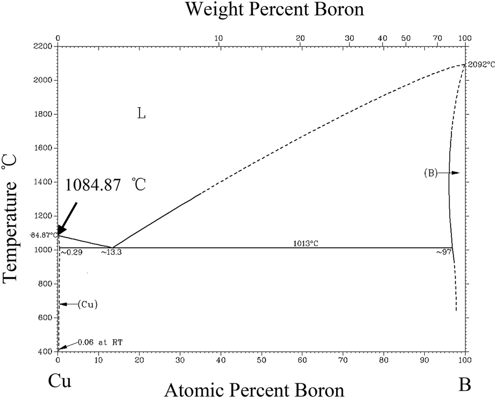 | ||
| Fig. 1 Cu–B phase diagram.21,22 | ||
Fig. 2 shows a schematic description of the system used for the synthesis of the boron nanotubes. Based on the alloy analysis, the Cu–B–nitric acid system was used, with Cu acting as the alloy environment, B as the carrier of the boron nanostructures and nitric acid solution as the extracted solution. First, we prepared Cu–B alloys by the direct melt reaction process, which were then were melted and cooled at a high cooling rate. The Cu–B alloy can be greatly refined by rapid solidification, and the size of boron in the Cu–B alloy can also be controlled and changed by different cooling rates and boron contents. Then, as the Cu was removed by erosion using nitric acid solution, boron tubes were obtained by centrifugation.
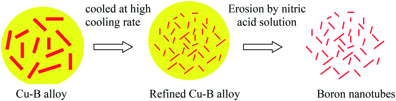 | ||
| Fig. 2 A schematic description of the system used for the synthesis of boron nanotubes. | ||
The crystallization conditions of boron in the Cu alloy can be changed by solidification of the Cu–B system. By changing the components and cooling rate, boron tubes with different sizes were obtained, as shown in Fig. 3. Fig. 3(a) shows an SEM image of the Cu-3 wt% B alloy after cooling at a rate of about 103 K s−1, in which the cross-section of the primary boron is a parallelogram. Boron tubes with micron sized cross-sections extracted from the alloy are shown in Fig. 3(b), from which it is clear that the center of the boron tube is hollow. Fig. 3(c) shows an SEM image of the Cu-1.5 wt% B alloy obtained at a cooling rate of about 20 K s−1. Even in this case, the cross-section of eutectic boron can be observed, which shows that the eutectic boron is hollow. Boron tubes with submicron sized cross-sections extracted from the alloy are shown in Fig. 3(d). Since some of the boron tubes are split, the presence of hollow tubes can be observed. A higher cooling rate leads to a smaller size for the boron tubes obtained. When the cooling rate was increased to about 105 K s−1, as shown in Fig. 3(e), the size of the boron nanotubes was closely related to the composition of the alloy. The boron nanotubes obtained from the hypoeutectic Cu–B alloy (Cu-1 wt%) were smaller than that obtained from the hypereutectic Cu–B alloy (Cu-3 wt% B). The boron nanotubes in Cu-3wt% B were typically all straight and several microns in length with diameters ranging between 50 and 500 nm. The HRTEM image of a typical boron nanotube obtained in Cu-1 wt% B is shown in Fig. 3(f), which highlights its multiwall structure. The sheets of the boron nanotubes are evident and the interlayer spacing between the sheets was found to be about 0.32 nm, which is consistent with the boron interlayer space in Liu's experimental results (0.32 nm)21 and very close to the theoretical values of 2.997 or 3.021 Å.21 The inner and outer diameters of the layered tubular structure were found to be 6 and 13 mm, respectively.
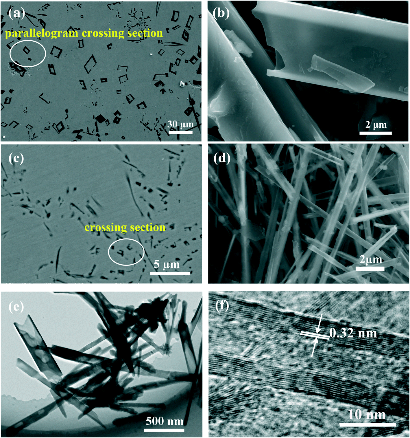 | ||
| Fig. 3 Boron tubes changed from about 15 nm to several tens of microns in the Cu–B system. (a) SEM image of the Cu-3 wt% B alloy cooled at a rate of about 103 K s−1; (b) micron size boron tubes extracted from the alloy in Fig. 3(a); (c) SEM image of Cu-1.5 wt% B alloy cooled at a rate of about 20 K s−1; (d) submicron size boron tubes extracted from the alloy in Fig. 3(c); (e) boron nanotubes extracted from Cu-3 wt% B cooled at a rate of about 105 K s−1 and (f) boron nanotubes extracted from Cu-1 wt% B cooled at a rate of about 105 K s−1. | ||
The chemical composition and crystal structure of the boron nanotubes were analyzed via STEM and TEM. The Cu-1.5 wt% B alloy cooled at a rate of about 105 K s−1 was reduced by long shear thinning and observed under a ZEISS LIBRA 200FE microscope, as shown in Fig. 4(a). Boron nanotubes with sizes ranging between 10 and 20 nm are observed in the Cu matrix and distributed at the Cu grain boundary, similarly to the eutectic boron in the Cu-1.5 wt% B alloy. A representative EELS spectrum obtained from a boron nanotube in Fig. 4(a) is shown in Fig. 4(b), which shows a high-intensity boron core-loss peak at about 200 eV and no Al, Cu and C peaks were detected. The boron nanotubes were extracted from the alloys and analyzed by EDX. A typical EDX spectrum of a boron nanotube (Fig. 4(c)) is shown in Fig. 4(d). According to the tests repeated more than 10 times, elemental O, Al and Cu could only be detected in small quantities. The EELS and EDX analyses therefore confirm that the phases obtained in the Cu alloy are boron nanotubes.
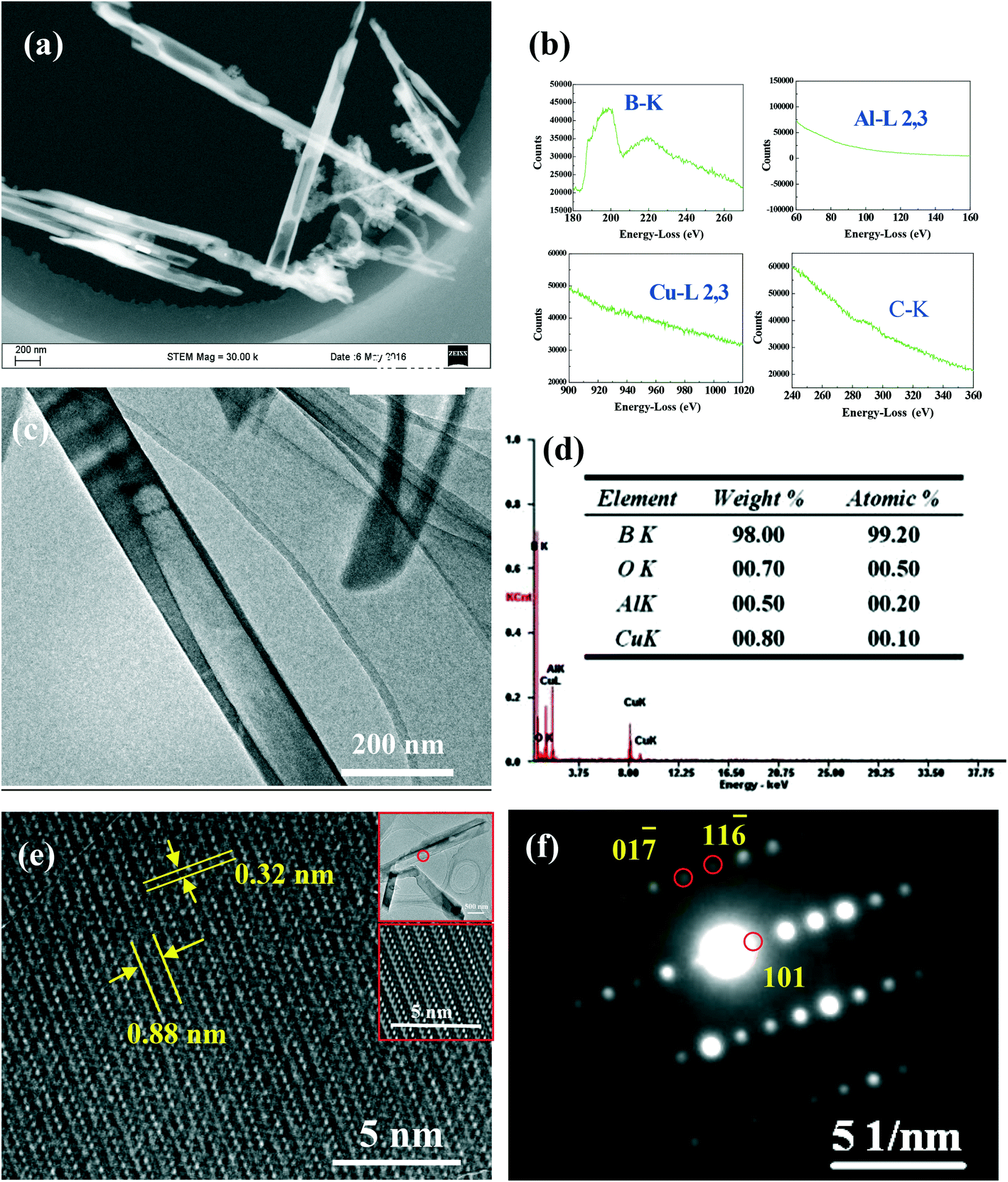 | ||
Fig. 4 Characterization of boron nanotubes in Cu alloy. (a) STEM image of Cu-1.5 wt% B cooled at a rate of about 105 K s−1; (b) EELS analysis of the boron nanotubes in the Cu alloy; (c) image of an extracted boron nanotube; (d) EDX analysis of the boron nanotubes; (e) HRTEM images of a boron nanotube and the inserted boron tube image; and (f) corresponding electron diffraction pattern along the [1![[7 with combining macron]](https://www.rsc.org/images/entities/char_0037_0304.gif) ![[1 with combining macron]](https://www.rsc.org/images/entities/char_0031_0304.gif) ] zone. ] zone. | ||
Two types of crystal boron nanostructures have been reported in the past, tetragonal9–11,21 and rhombohedral.4,30 To analyze the detailed crystalline structure of the boron nanotubes in the Cu alloy, HRTEM was employed. A typical TEM image of a boron nanotube is shown in Fig. 4(e) in which it can be found that the boron nanotube has clear lattice fringes. The TEM images and their corresponding electron diffraction patterns are shown in Fig. 4(e) and (f). Fig. 4(e) shows a high-resolution TEM image of a boron tube which is shown in the inserted image, and the HRTEM image location is labeled as a red circle in the inserted image. Fig. 4(f) shows the corresponding electron diffraction pattern of Fig. 4(e), along the [1] zone. According to the TEM analysis, the crystal structure of the boron tubes is closer to β-rhombohedral, thus the boron tubes prepared in this work are β-rhombohedral structures. Combining the HRTEM results we concluded that the boron nanotubes in this work are perfect single crystals with a β-rhombohedral structure, which is in agreement with the data of the Joint Committee for Powder Diffraction Standards (JCPDS) card PDF#31-0207 (a = b = 1.0925 nm and c = 2.3814 nm).
Given the difficulty to synthesize boron nanostructures, particularly in the form of nanotubes, it is worth investigating the reasons why they can be formed in the Cu alloy. In the present work, the liquid structure of the Cu–B system was studied in order to understand and explain this phenomenon. Fig. 5(a) shows the partial correlation functions of the Cu80B20 alloy at 1673 K. It is observed clearly that the first peak of the gBB(r) curve is much higher than that of the other g(r) curves, which indicates that the affinity of the B–B pair is the strongest one among those reported. Moreover, the gBB(r) curve between the first and second peaks is very deep and presents high ordering of the B–B pairs, which indicate a solid-like cluster in the liquid. Fig. 5(b) shows the pair-distribution functions of the B–B pairs at different temperatures. With a decrease in temperature, the nearest neighbor peak of the B–B pair is higher and sharper, which directly implies that the interatomic force of the B–B pair increases and that the ordered regions are extended to lower temperatures. Furthermore, we calculated the chemical environment of the Cu–B system at 1673 K, as shown in Table 1. It can be found that calculated coordination number ratios of CuCu (0.87) and BB (0.21) are larger than their nominal values (0.80 and 0.20, respectively), whereas the calculated coordination number ratios of CuB (0.13) and BCu (0.79) are smaller than their nominal values (0.20 and 0.80, respectively). On the basis of the above analysis, it can be deduced that the Cu atoms tend to combine with Cu atoms and B atoms tend to combine with B atoms in the Cu–B system. There is hardly any attractive force between the Cu and B atoms, whereas the repulsion force is very strong.
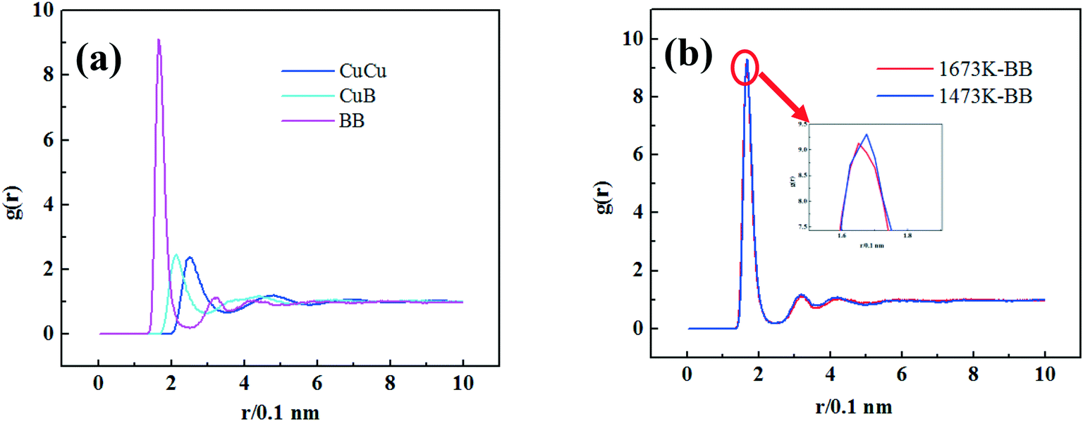 | ||
| Fig. 5 Partial pair correlation functions of the Cu80B20 system. (a) Partial correlation functions of the Cu80B20 alloy at 1673 K. (b) Pair-distribution functions of the B–B pairs at 1473 K and 1673 K. | ||
| Term | Partial coordination number | Calculated coordination number ratio | Nominal coordination number ratio |
|---|---|---|---|
| CuCu | 10.97 | 0.87 | 0.80 |
| CuB | 1.60 | 0.13 | 0.20 |
| BCu | 6.42 | 0.79 | 0.80 |
| BB | 1.65 | 0.21 | 0.20 |
The molecular dynamics method was then used to study the growth of the boron nanotubes in the Cu alloy. The study initially addressed the solidification behavior of the boron atoms on the (111), (110) and (100) planes of Cu, as shown in Fig. 6(a). The corresponding energy change is shown in Fig. 6(b). The results show that the boron atoms form a film on the (111) plane and a boron nanotube could be formed if the boron film coiled; however, it is easier for the boron atoms to coil on the (110) and (100) planes, especially on the (100) plane. Since the coil behavior is beneficial to the formation of boron nanotubes, the Cu environment is very important for the formation of boron nanotubes in the Cu alloy.
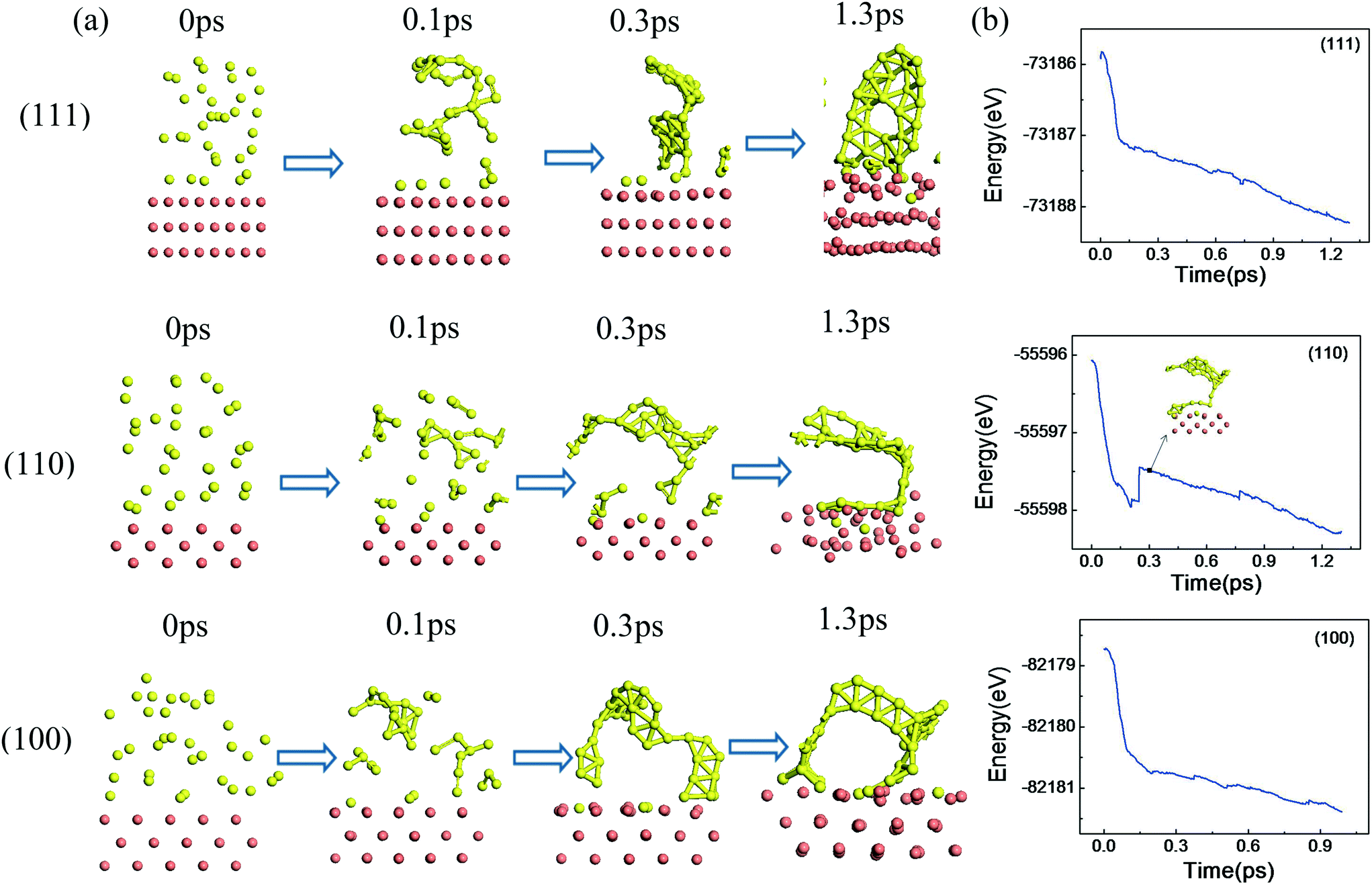 | ||
| Fig. 6 Solidification of boron atoms on the plane of Cu. (a) Solidification of boron atoms on the (111), (110) and (100) planes of Cu, i.e. red spheres are Cu atoms and the yellow spheres are boron atoms and (b) the corresponding energy change. | ||
Since it is easy for boron to aggregate in the gap of Cu crystals, we simulated the structural evolution of the boron atoms in the one dimensional confined space of crystal Cu to study the role of Cu on the formation of boron nanotubes, as shown in Fig. 7.
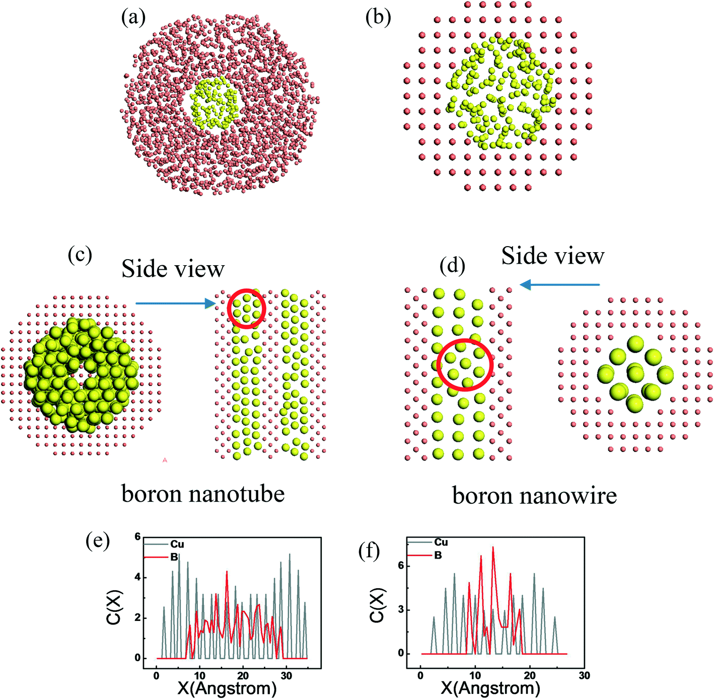 | ||
| Fig. 7 Structural evolution of boron atoms in the one dimensional confined space of crystal Cu. (a) Boron atoms solidified in Cu melt. (b) Boron atoms solidified in crystal Cu. (c) Boron nanotubes formed in crystal Cu and their cross-sectional view. (d) Boron nanowires formed in crystal Cu and their cross-sectional views. (e) Atomic concentration distribution curve of Cu–boron nanotubes. (f) Atomic concentration distribution curve of Cu–boron nanowires. | ||
The melting point of a small amount of linear arrayed boron atoms is lower than that of blocky boron because of size effects. On the other hand, the melting point of the Cu matrix is close to that of blocky Cu. As a consequence, a condition exists in which Cu has solidified but boron in the Cu crystal has not, as shown in Fig. 7(a) and (b). When Cu atoms are present in the center of the boron melt, the solidified boron is filled by Cu crystals and forms boron nanotubes, as shown in Fig. 7(c). On the other hand, in the absence of Cu atoms in the boron melt, the boron atoms solidify in the form of nanowires, as shown in Fig. 7(d). Although defects are present in the crystal structure of the boron nanotubes and boron nanowires, their lattice structure is similar to the HRTEM observation. The atomic concentration distribution curves of the Cu–boron nanotubes are reported in Fig. 7(e), in which the B and Cu concentration distributions are shown in red and gray, respectively According to the measurements, the stable concentration distribution peak spacing of Cu atoms is 2 Å, which is close to the lattice spacing of the Cu (200) plane, which is in accordance with the analysis of Fig. 5. The boron concentration distribution peak spacing is between 1.5 and 3 Å, which shows that the boron atom distributions in the nanotubes and nanowires are not regular and have certain structural defects.
Finally boron nanotubes (BNT(3,3))16 were used as nuclei and their growth was simulated, as shown in Fig. 8. Given that the adsorption energy between B atoms is larger than that between Cu and B, the boron atoms aggregate and form a regular tube structure around the boron nanotubes. The new boron nanotube then induces another regular arrangement of boron atoms, so that a multilayer boron nanotube is formed, as shown in Fig. 8(a). According to the simulation, however, the force between the inner and outer atoms decreases with an increase in the number of layers. The layered structure is no longer observed clearly when the number of layers exceeds four, which indicates that the expansion of the boron nanotubes cannot continue indefinitely. The evolution of the layers was also studied, as shown in Fig. 8(b). It can be seen that the round layers are not stable and transformed into a parallelogram before solidifying in the crystal state.
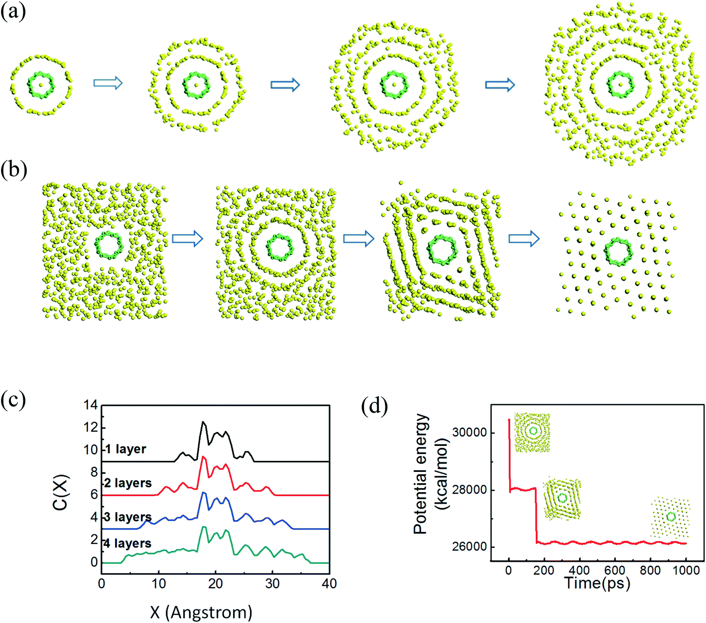 | ||
| Fig. 8 Growth of boron nanotubes simulated by molecular dynamics. (a) Growth of a multilayer boron nanotube. (b) Growth of boron nanotubes with long time relaxation. (c) Evolution of atomic concentration distribution with an increase in layers in Fig. 8(a). (d) Corresponding energy change from which it can be seen that the energy of the parallelogram is lower than that of the round nanotube. | ||
Fig. 8(c) shows the evolution of atomic concentration distribution with an increase in layers, which further confirms the above conclusion. Moreover, according to the measurement of peak spacing of atomic concentration distribution, it can be found that the layer spacing is about 3–3.5 Å, which is consistent with the experimental results shown in Fig. 3(f). The corresponding energy change is shown in Fig. 8(d), where it can be seen that the energy of the parallelogram is lower than that of the round nanotubes, which is in agreement with the experimental observations summarized in Fig. 3.
Based on the experimental observations and computer simulations of the Cu–B system, the growth mechanism of boron nanotubes in the Cu alloy is proposed. In conditions in which Cu solidifies first, the growth mechanism can be divided into four stages, as depicted in Fig. 9. Stage 1: when Cu solidifies, B separates and surrounds the solidified Cu. Stage 2: the separated B atoms aggregate and form clusters surrounding the solidified Cu followed by further aggregation of the B clusters. Meanwhile, Cu clusters also move towards the solidified Cu. Stage 3: when the surrounding boron reaches a threshold concentration, the boron nanostructure folds and forms a nanotube. At this stage, the Cu atoms can only transfer through the opening of the boron nanotubes, whereas the B atoms can transfer from both the outside and the opening of the boron nanotubes. The assembly of boron at the opening causes the boron nanotubes to grow quickly along the [0001] direction, while the assembly of boron atoms outside increases the wall thickness of the nanotubes. Stage 4: according to the thermodynamic principle of crystal growth and Wulff's theorem, the equilibrium shape of a crystal is the shape with the minimum total surface energy, and the faces with lower surface energy will be exposed.31,32 If more time is available for the Cu and B atoms to aggregate, the cylinder is not stable and surface selection will occur. The crystal structure of the boron nanotubes belongs to the R![[3 with combining macron]](https://www.rsc.org/images/entities/char_0033_0304.gif) m-no.166 crystal group, and can be converted into the double centered hexagonal crystal lattice (a = b ≠ c, α = β = 90°, γ = 120°), in which the {001} crystalline planes have the highest growth rate and the preferential growth direction is [0001]. According to the atomic arrangement along the [0001] direction, quadrangular boron tubes may form during the non-equilibrium solidification. According to the calculation in Fig. 5, the affinity of the B–B pair is very strong, thus when B solidifies first the growth mechanism is different and the cooling rate plays a key role. If the cooling rate increases, the low diffusion rate favors the growth of defects in the boron phase and allows Cu solidification. The subsequent growth pattern of the boron tube goes to stage 4 directly, which justifies the observed presence of closed micro-nano boron. Hoek et al. analyzed the thermal dynamic conditions that favor the formation of hollow tube structures and identified the concentration range in which they are stable.33 Wu et al. studied the relationship between crystal morphology, growth mechanism, growth rate and driving force and showed that hollow structures may form because of Klinkenberg effects.34 The boron nanotubes in the Cu alloy can therefore be considered as skeleton crystals,35 and the formation of boron nanotubes is closely related with the structural characterization of the Cu–B alloy, which, in turn, is affected by the cooling rate and boron concentration. The composition is closely related to the boron tube size. First, because Cu–B has a eutectic phase diagram, the composition can determine if the boron is eutectic boron or primary boron in the Cu–B system since the size of eutectic boron is much smaller than that of primary boron. Second, boron tubes can be formed when the composition and cooling rate are matched. If the boron tube is primary boron under the same cooling rate, the boron tubes have smaller size with lower composition of the alloy. If the boron tubes have the same composition, they will have a smaller size with a higher cooling rate. Moreover, the match relationship plays a key role in formation of boron tubes in the Cu–B system.
m-no.166 crystal group, and can be converted into the double centered hexagonal crystal lattice (a = b ≠ c, α = β = 90°, γ = 120°), in which the {001} crystalline planes have the highest growth rate and the preferential growth direction is [0001]. According to the atomic arrangement along the [0001] direction, quadrangular boron tubes may form during the non-equilibrium solidification. According to the calculation in Fig. 5, the affinity of the B–B pair is very strong, thus when B solidifies first the growth mechanism is different and the cooling rate plays a key role. If the cooling rate increases, the low diffusion rate favors the growth of defects in the boron phase and allows Cu solidification. The subsequent growth pattern of the boron tube goes to stage 4 directly, which justifies the observed presence of closed micro-nano boron. Hoek et al. analyzed the thermal dynamic conditions that favor the formation of hollow tube structures and identified the concentration range in which they are stable.33 Wu et al. studied the relationship between crystal morphology, growth mechanism, growth rate and driving force and showed that hollow structures may form because of Klinkenberg effects.34 The boron nanotubes in the Cu alloy can therefore be considered as skeleton crystals,35 and the formation of boron nanotubes is closely related with the structural characterization of the Cu–B alloy, which, in turn, is affected by the cooling rate and boron concentration. The composition is closely related to the boron tube size. First, because Cu–B has a eutectic phase diagram, the composition can determine if the boron is eutectic boron or primary boron in the Cu–B system since the size of eutectic boron is much smaller than that of primary boron. Second, boron tubes can be formed when the composition and cooling rate are matched. If the boron tube is primary boron under the same cooling rate, the boron tubes have smaller size with lower composition of the alloy. If the boron tubes have the same composition, they will have a smaller size with a higher cooling rate. Moreover, the match relationship plays a key role in formation of boron tubes in the Cu–B system.
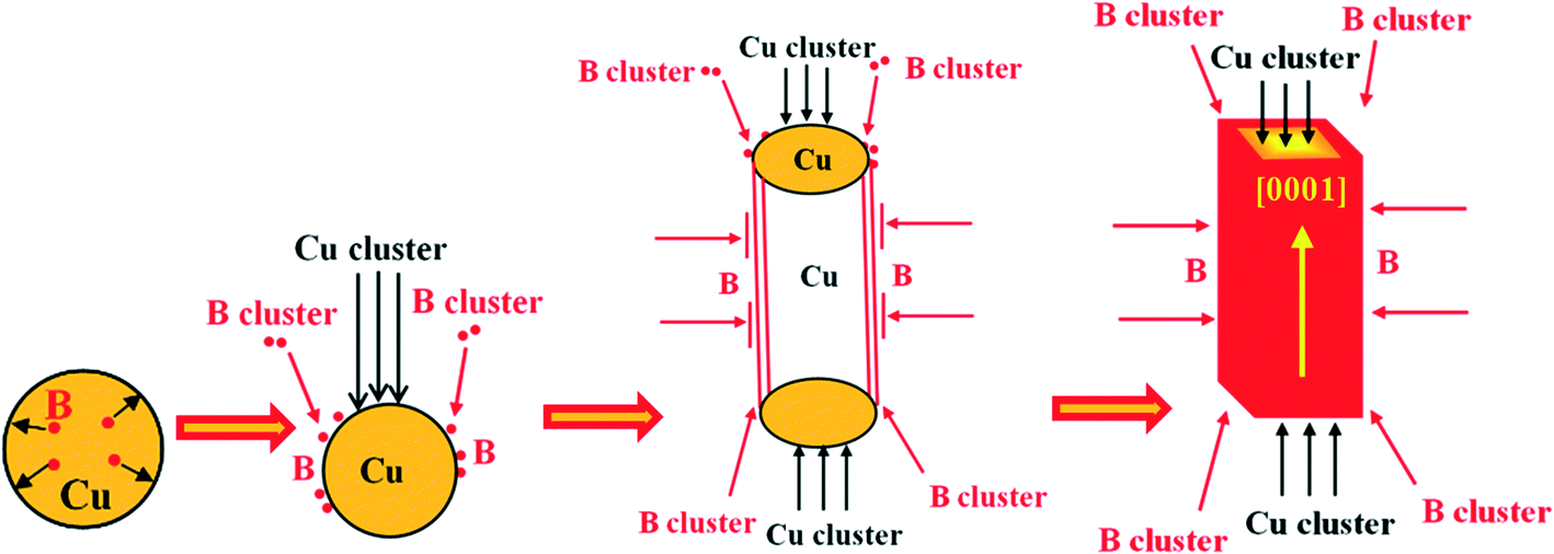 | ||
| Fig. 9 Schematic of the growth mechanism of boron nanotubes in the Cu–B system. | ||
Conclusions
In summary, boron nanotubes have been prepared via a novel method, which are closely related to the unique structure of the Cu–B system. The boron nanotubes are perfect single crystals with a β-rhombohedral structure and their size can be controlled and changed from about tens to several hundreds of nanometers. The combined experimental and dynamic simulation results led to the conclusion that the Cu crystal environment is very important for the formation of boron nanotubes. In addition, the round layers of boron nanotubes are not stable and tend to transform into a parallelogram, which is characterized by a lower energy content.Acknowledgements
This work is supported by the National Basic Research Program of China (973 Program, Grant number: 2012CB825702), National Natural Science Foundation of China (Grant number: 51001065) and the Young Scholars Program of Shandong University (YSPSDU).Notes and references
-
R. M. Adams, Boron, Metallo-Boron, Compounds and Boranes, Interscience Publishers, New York, USA, 1964 Search PubMed
.
- A. J. Mannix, X. F. Zhou, B. Kiraly, J. D. Wood, D. Alducin, B. D. Myers, X. L. Liu, B. L. Fisher, U. Santiago, J. R. Guest, M. J. Yacaman, A. Ponce, A. R. Oganov, M. C. Hersam and N. P. Guisinger, Science, 2015, 350, 1513–1516 CrossRef CAS PubMed
- L. Cao, Z. Zhang, L. Sun, C. Gao, M. He, Y. Wang, Y. Li, X. Zhang, G. Li, J. Zhang and W. Wang, Adv. Mater., 2001, 13, 1701–1704 CrossRef CAS
- Y. Q. Wang and X. F. Duan, Appl. Phys. Lett., 2003, 82, 272–274 CrossRef CAS
- X. M. Meng, J. Q. Hu, Y. Jiang, C. S. Lee and S. T. Lee, Chem. Phys. Lett., 2002, 370, 825–828 CrossRef
- Y. Zhang, H. Ago, M. Yumura, T. Komatsu, S. Ohshima, K. Uchida and S. Iijima, Chem. Commun., 2002, 2806–2807 RSC
- C. J. Otten, O. R. Lourie, M. F. Yu, J. M. Cowley, M. J. Dyer, R. S. Ruoff and W. E. Buhro, J. Am. Chem. Soc., 2002, 124, 4564–4565 CrossRef CAS PubMed
- Y. Y. Wu, B. Messer and P. D. Yang, Adv. Mater., 2001, 13, 1487–1489 CrossRef CAS
- Z. K. Wang, Y. Shimizu, T. Sasaki, K. Kawaguchi, K. Kimura and N. Koshizaki, Chem. Phys. Lett., 2003, 368, 663–667 CrossRef CAS
- X. J. Wang, J. F. Tian, T. Z. Yang, L. H. Bao, C. Hui, F. Liu, C. M. Shen, N. S. Xu and H. J. Gao, Adv. Mater., 2007, 19, 4480–4485 CrossRef CAS
- T. T. Xu, J. G. Zheng, N. Q. Wu, A. W. Nicholls, J. R. Roth, D. A. Dikin and R. S. Ruoff, Nano Lett., 2004, 4, 963–968 CrossRef CAS
- M. Bechelany, A. Brioude, P. Stadelmann, S. Bernard, D. Cornu and P. Miele, J. Phys. Chem. C, 2008, 112, 18325–18330 CAS
- M. Weber, B. Koonkaew, S. Balme, I. Utke, F. Picaud, I. Iatsunskyi, E. Coy, P. Miele and M. Bechelany, ACS Appl. Mater. Interfaces, 2017, 9, 16669–16678 CAS
- H. J. Zhai, B. Kiran, J. Li and L. S. Wang, Nat. Mater., 2003, 2, 827–833 CrossRef CAS PubMed
- W. Huang, A. P. Sergeeva, H. J. Zhai, B. B. Averkiev, L. S. Wang and A. I. Boldyrev, Nat. Chem., 2010, 2, 202–206 CrossRef CAS PubMed
- X. B. Yang, Y. Ding and J. Ni, Phys. Rev. B, 2008, 77, 041402 CrossRef
- I. Boustani, A. Rubio and J. A. Alonso, Chem. Phys. Lett., 1999, 311, 21–28 CrossRef CAS
- A. Gindulyte, W. N. Lipscomb and L. Massa, Inorg. Chem., 1998, 37, 6544–6545 CrossRef CAS PubMed
- I. Boustani, A. Quandt, E. Hernμndez and A. Rubio, J. Chem. Phys., 1999, 110, 3176–3185 CrossRef CAS
- D. Ciuparu, R. F. Klie, Y. Zhu and L. Pfefferle, J. Phys. Chem. B, 2004, 108, 3967–3969 CrossRef CAS
- F. Liu, C. Shen, Z. Su, X. Ding, S. Deng, J. Chen, N. Xu and H. Gao, J. Mater. Chem., 2010, 20, 2197–2205 RSC
- S. Carenco, D. Portehault, C. Boissière, N. Mézailles and C. Sanchez, Chem. Rev., 2013, 113, 7981–8065 CrossRef CAS PubMed
- Y. Y. Wu, C. Li, X. F. Liu and K. Lu, J. Alloys Compd., 2012, 527, 184–187 CrossRef CAS
- G. Kresse and J. Furthmüller, Comput. Mater. Sci., 1996, 6, 15–50 CrossRef CAS
- L. Pauling, J. Am. Chem. Soc., 1932, 54, 3570–3582 CrossRef CAS
- S. Nosé, J. Chem. Phys., 1984, 81, 511–519 CrossRef
- A. K. Rappe, K. S. Colwell and C. J. Casewit, Inorg. Chem., 1993, 32, 3438–3450 CrossRef CAS
- D. J. Chakrabarti and D. E. Laughlin, Bull. Alloy Phase Diagrams, 1982, 3, 45–48 CrossRef
- J. Rexer and G. Petzow, Metall., 1970, 24, 1083–1086 CAS
- H. Werheit, V. Filipov, U. Kuhlmann, T. Dose and T. Lundstrom, Solid State Sci., 2015, 47, 7–12 CrossRef CAS
-
M. C. Flemings, Solidification processing, McGraw-Hill, New York, 1974 Search PubMed
- G. H. Liu, K. X. Chen, H. P. Zhou, J. J. Tian, C. Pereira and J. M. F. Ferreira, Cryst. Growth Des., 2006, 6, 2404–2411 CAS
- B. Van der Hoek, J. P. Van der Eerden and P. Bennema, J. Cryst. Growth, 1982, 56, 621–632 CrossRef CAS
- Y. S. Wu, K. Pruess and P. Persoff, Transp. Porous Media, 1998, 32, 117–137 CrossRef CAS
- M. King, A. Bowen, K. Brinsko and S. Sparenga, Microscope, 2008, 56, 125–130 CAS
Footnote |
| † Electronic supplementary information (ESI) available. See DOI: 10.1039/c7ce00818j |
| This journal is © The Royal Society of Chemistry 2017 |