
Efficient pure green emission from Er-doped Ga2O3 films
Zhengwei
Chen
,
Katsuhiko
Saito
,
Tooru
Tanaka
and
Qixin
Guo
 *
*
Department of Electrical and Electronic Engineering, Synchrotron Light Application Center, Saga University, Saga 840-8502, Japan. E-mail: guoq@cc.saga-u.ac.jp; Fax: +81 952 28 8651; Tel: +81 952 28 8662
First published on 5th July 2017
Abstract
This study briefly reviews effect of the doping content on the structure, surface morphology, and optical properties of Er-doped Ga2O3 films on sapphire and Si substrates grown via pulsed laser deposition. Temperature insensitive pure green luminescence has been demonstrated from these films. We succeeded in fabricating light-emitting devices (LEDs) based on Ga2O3:Er/Si heterojunctions. Bright pure green emission can be observed by the naked eye from the LEDs. The driven voltage of these LEDs is 6.2 V, which is lower than those of ZnO:Er/Si and GaN:Er/Si devices. In addition, we determined the values of the valence band offset and conduction band offset of the Ga2O3/Si heterojunctions. The results obtained in this study shall provide a useful guideline for the development of Si-based green LEDs using Ga2O3 as the host materials for Er3+ ions.
 Zhengwei Chen | Zhengwei Chen received a B.E. from Tianjin Polytechnic University, China, in 2011. He received M.E. and Ph.D. degrees in electrical and electronic engineering from Saga University, Japan, in 2014 and 2017, respectively. In 2017, He joined the School of Science, at Beijing University of Posts and Telecommunications, China. His present research interests include characterization of compound semiconductors and fabrication of electronic devices. |
 Katsuhiko Saito | Katsuhiko Saito received B.S. and M.S. degrees in physics from Hirosaki University, Japan, in 1996 and 1998, respectively. He then received a Ph.D. degree in engineering from Tohoku University, Japan, in 2003. He then spent five and a half years as a Postdoctoral or Special-Appointment Researcher at Saga University, Japan. In 2009, he became an Assistant Professor at the Synchrotron Light Application Center, Saga University. His present research interests include epitaxial growth of wideband gap semiconductor materials, and micro- and nanostructure fabrication for device applications. |
 Tooru Tanaka | Tooru Tanaka received B.E., M.E., and Ph.D. degrees in electrical and electronic engineering from Toyohashi University of Technology, Japan, in 1995, 1997, and 2000, respectively. In 2000, he joined the Department of Electrical and Electronic Engineering, Saga University, Japan, as an Assistant Professor. He then became an Associate Professor in 2009 and Full Professor in 2015. His current research interests include molecular beam epitaxial growth of II–VI-O dilute oxides and related materials for the application to next-generation optoelectronic devices. Dr. Tanaka has published more than 150 journal papers and book chapters. |
 Qixin Guo | Qixin Guo received B.E., M.E., and Ph.D. degrees in electrical and electronic engineering from Toyohashi University of Technology, Japan. He joined the Department of Electrical and Electronic Engineering, Saga University, Japan, as an Assistant Professor in 1992, and then became an Associate Professor in 1997 and Full Professor in 2007. He has also been a Member of the Saga University Synchrotron Light Application Center, where he is currently the director. His current research interests include epitaxial growth of compound semiconductors and synchrotron light applications in novel material sciences. Dr. Guo has published over 270 journal papers and book chapters. |
1. Introduction
Pure green emission (∼550 nm) devices play an important role in full-color display technology and in the development of white light-emitting devices (LEDs).1 Nakamura et al. have demonstrated green emission with InGaN alloys and quantum well structures. However, this configuration is expensive and the device architectures are highly complicated, thus limiting their applications.2 Recently, Er-doped wide bandgap semiconductor devices have received extensive attention because of their low-cost, simple production, and temperature insensitive pure green emission.3 Wu et al. have investigated the structural and optical characteristics of a Er-doped GaN powder and observed green emission from it.4 Birkhahn and Steckl have observed green emission at 537 and 558 nm from Er-doped GaN films grown on Si.5 Er-doped III-N double heterostructure LEDs and their electroluminescence (EL) properties have been reported by Zavada et al.6 In addition, Harako et al. have fabricated a n-ZnO:Er/p-Si LED and obtained intense green emission from it at room temperature.7 All these semiconductors exhibit strong and sharp green emission due to intra-4f-shell transitions in the Er ion cores and have potential applications in color displays and luminescence devices.4–8 Favennec et al. have demonstrated that the luminescence efficiency of dopant emission can be highly improved using a wide bandgap host.9 Furthermore, Steckl et al. have reported that wide bandgap semiconductors exhibit high thermal and chemical stabilities that make them ideal hosts for RE ions.10 Monoclinic Ga2O3 is a potential candidate due to its direct and wide bandgap (∼4.9 eV) and physical and chemical stabilities.11–14 In this study, we briefly reviewed the effect of the doping content on the structure, surface morphology, and optical properties of Er-doped Ga2O3 films on sapphire and Si substrates as well as bright green LEDs based on Ga2O3:Er/Si heterojunctions.15,16 We also analyzed the transfer energy process by investigating the band offset of the heterojunction interface.172. Er-doped Ga2O3 films on sapphire
Sapphire is a material with a unique combination of physical, chemical, and optical properties that makes it resistant to high temperature, thermal shock, water and sand erosion, and scratching. It is a superior window material for the growth of III–V and II–VI compounds, such as GaN, for blue LEDs and laser diodes.18 First, we epitaxially grew Ga2O3 films on the sapphire substrate with different Er contents.The Er-doped Ga2O3 films were grown on (0001) sapphire substrates by a pulsed laser deposition (PLD) method using a KrF excimer laser source. Bulk (diameter of 20 mm) samples with different Er contents (xt) were used as targets. High purity oxygen gas (99.9999%) was introduced through mass flow controllers after the pressure of the chamber was evacuated to below 5 × 10⁻⁶ Pa. The oxygen pressure was set at 1 × 10⁻¹ Pa, whereas the substrate temperature was set at 500 °C. X-ray photoelectron spectroscopy (XPS) measurements were performed using an Al Kα X-ray source. Structural properties of the films were evaluated via conventional θ–2θ scan X-ray diffraction (XRD) using the Kα emission line of copper. The surface morphology and roughness of the films were studied using an atomic force microscope (AFM) on 2 × 2 μm areas. Photoluminescence (PL) measurements were performed using an Ar laser operating at a wavelength of 488 nm as the excitation source.
Fig. 1(a) reveals the high resolution XPS spectra of the Er 4p peak centered at 321.6 eV. The intensity of the Er peak increases with the increasing Er content. The Er content in Ga2O3 films has been obtained from the XPS spectra after applying an atomic sensitivity factor and is shown in Fig. 1(b) as a function of the Er content of the targets. We found that the Er content in the films increased almost linearly with the increasing Er content of the targets. This suggests that the Er contents in the Ga2O3 films can be controlled by adjusting the Er content in the targets.
 | ||
| Fig. 1 (a) Er 4p core level spectra of Ga2O3 films with different Er contents in the targets. (b) Er contents in the films as a function of the Er contents of the targets.15 | ||
Fig. 2 shows the XRD patterns of the Ga2O3 films with different Er contents. Herein, three peaks were clearly observed at 18°, 38°, and 58°, which could be assigned to the (−201), (−402), and (−603) planes of Ga2O3, respectively, by comparing the measured diffraction data with the known diffraction peaks listed in the International Center for Diffraction Data catalog.13 These results indicated an epitaxial relationship where the (−201) plane of Ga2O3 is parallel to the (0001) plane of the sapphire substrate. We found that with the increasing Er content, the peaks slightly shifted to lower diffraction angles, as exemplified by the (−402) peak in Fig. 2(b); this indicates an increase in the lattice constant, which is due to the fact that the ion radius of Er3+ (0.88 Å) is larger than that of Ga3+ (0.62 Å). The incorporation of Er into Ga2O3 in a way that Er3+ substitutes Ga3+ increases the lattice constants of Ga2O3; as a result, the diffraction peaks shift to lower angles.19 Note that the (004) peak of Ga2O3 appears for the Er-doped Ga2O3 samples. This is ascribed to the significant difference between the ionic radii of Er and Ga. The incorporation of Er into the Ga2O3 film leads to the degradation of crystal quality.12
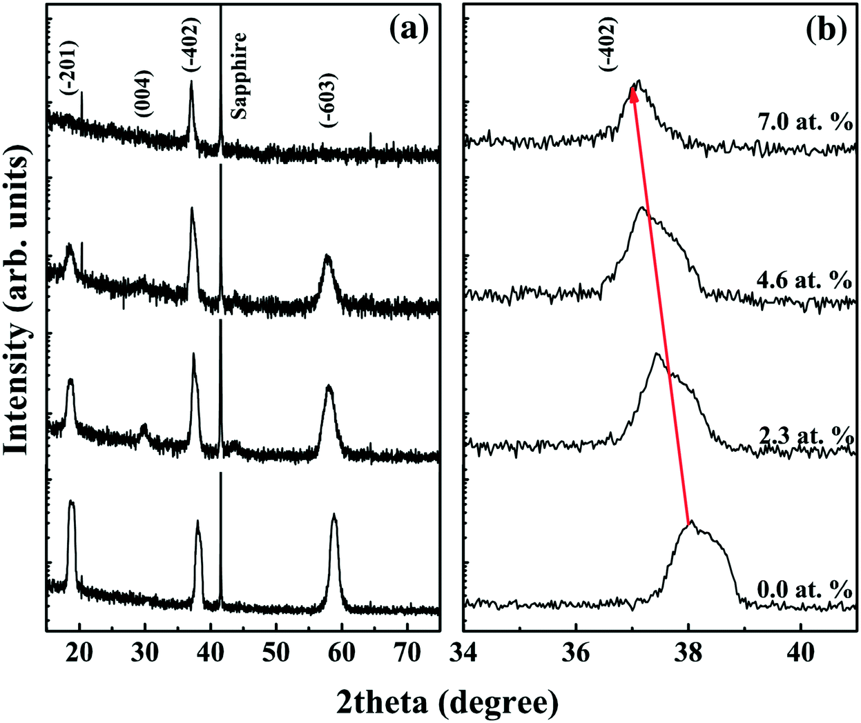 | ||
| Fig. 2 (a) XRD patterns of the Ga2O3 thin films with different Er doping contents in the film (x). (b) The corresponding XRD profiles of the near (−402) peaks.15 | ||
Fig. 3 shows the 2 × 2 μm AFM images for Ga2O3 thin films with different Er doping contents. It is clear that the morphology changes with different Er doping contents. For the pure Ga2O3 film, island-like structures appear. As the Er content increases, the resulting morphology transforms from island structures to splitting slim needle-like structures. The root-mean-square (RMS) roughness provides an idea about the quality of the surface under investigation. It is known that thicker films often result in rougher surfaces.20 In this study, the thickness of all the samples was determined to be about 500–550 nm. The RMS roughness of the films with 0.0, 2.3, 4.6, and 7.0 at% Er content was found to be 3.4, 5.3, 7.4, and 8.9 nm, respectively. It is clear that the surface RMS roughness increases with the increasing Er-doping content; this suggests that the roughness difference in the present experiments is caused by Er doping into the Ga2O3 films. The maximum roughness of the films is below 9 nm, indicating that the films have a smooth surface.
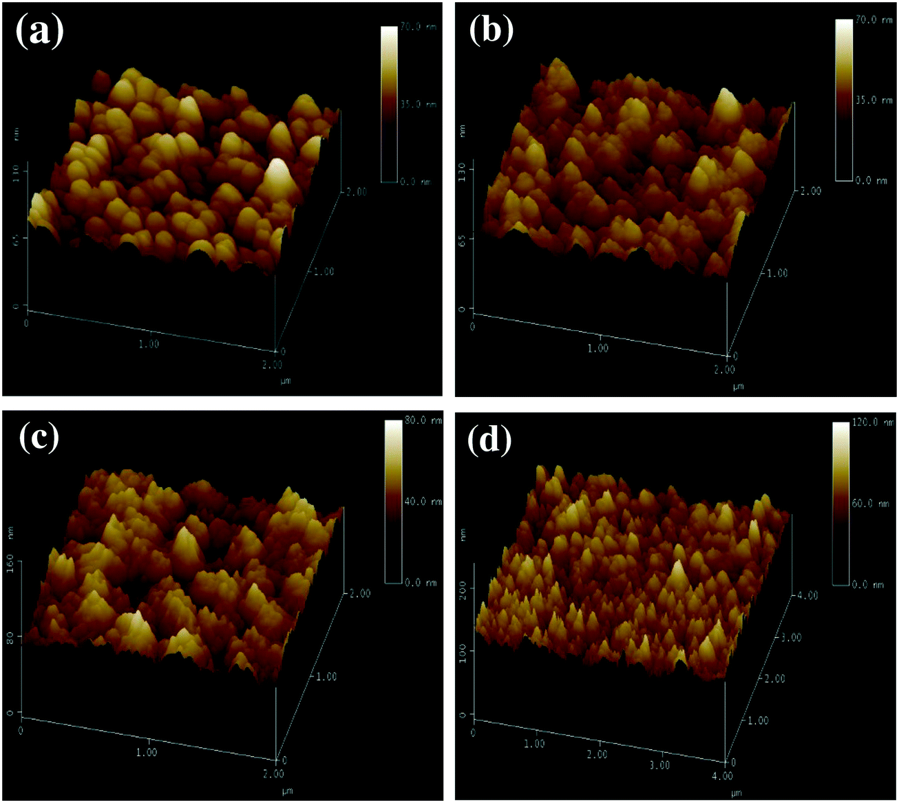 | ||
| Fig. 3 AFM images of the Ga2O3 films with different Er doping contents in the films: (a) 0.0, (b) 2.3, (c) 4.6, and (d) 7.0 at%.15 | ||
Fig. 4 shows the PL spectra of the Ga2O3 thin films with different Er contents acquired at room temperature. The PL spectra for the Er-doped Ga2O3 films demonstrate characteristic Er ion emission with the strongest peak at 550 nm caused by the 4S3/2 to 4I15/2 transition.10,15 The intensity of the pure green emission line observed at 550 nm remarkably increases with the increasing Er-doping content in the Ga2O3 films. The 550 nm emission peak with a shoulder at longer wavelength is ascribed to Stark splitting due to the spin–orbit splitting of the energy level.18 Other PL peaks observed at 524, 655, 850, and 975 nm can be assigned to the transitions from 2H11/2 to 4I15/2, 4F9/2 to 4I15/2, 4I9/2 to 4I15/2, and 4I11/2 to 4I15/2, respectively.13 In our study, the excitation energy of incident light used for the measurement is lower than the bandgap of Ga2O3. However, the electrons can be excited from the valence band to the donor band (oxygen vacancy) by this light source. The related energy due to the recombination of electrons in the defect state with the photogenerated holes can transfer to a resonant excitation of Er3+ ions with a 488 nm excitation wavelength, owing to 4I15/2 to 4F7/2 transition.21,22 Similar observations have been reported in Er-doped GaN films and Er-doped Ga2O3 bulk.3,21
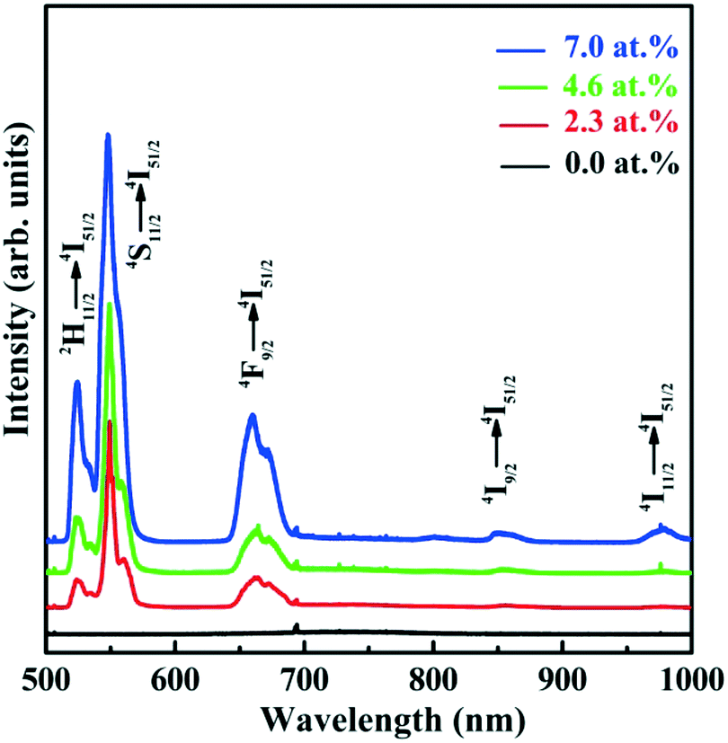 | ||
| Fig. 4 PL spectra of the Ga2O3 thin films with different Er doping contents in the film.15 | ||
Fig. 5(a)–(c) shows the temperature-dependent (TD) PL spectra of the Ga2O3 films with different Er contents obtained in the temperature range from 77 to 450 K. It is clear that no peak shifts at 550 nm in the PL spectrum for all the samples; however, the intensity of these emission lines at 550 nm monotonically decreases with the increasing temperature from 77 to 450 K, whereas the intensity of the 524 nm emission line appears and increases with the increase in temperature above 150 K. The most likely explanation for the opposite temperature dependence between two closely spaced electronic states is that electrons are thermally equilibrated between two levels.3 Moreover, it is interesting to compare the results obtained in this study with those obtained by Steckl et al. for Er-doped GaN films. It was found that the behavior of Er in GaN and Ga2O3 films was substantially similar.3 However, Fig. 5(d) summaries the normalized intensity as a function of temperature ranging from 77 to 450 K together with the reported data for the Er-doped GaN for comparison. The normalized intensity of the green emission at 550 nm decreases with the increasing temperature. Herein, note that the normalized intensity of the Er-doped Ga2O3 films is less affected by temperature as compared to that of Er doped GaN films. Favennec et al.9 and Neuhalfen et al.23 have demonstrated that the thermal quenching of the emission intensity is more severe for smaller bandgap materials, and wide bandgap compounds exhibit the least temperature dependence. This is because of the formation of defects and shrinkage of the distance between Er ions, or ion-defect cross relaxation that can cause photoluminescence quenching.24 Thermal quenching of the intra-4f Er luminescence efficiency can be reduced by choosing wide bandgap materials, in which the isoelectronic trap levels are deep.25 These results indicate that Ga2O3 is a better host material for Er than GaN, thus opening the possibility of applications of pure green luminescence devices based on Ga2O3 using Er as a dopant in a wide temperature range.
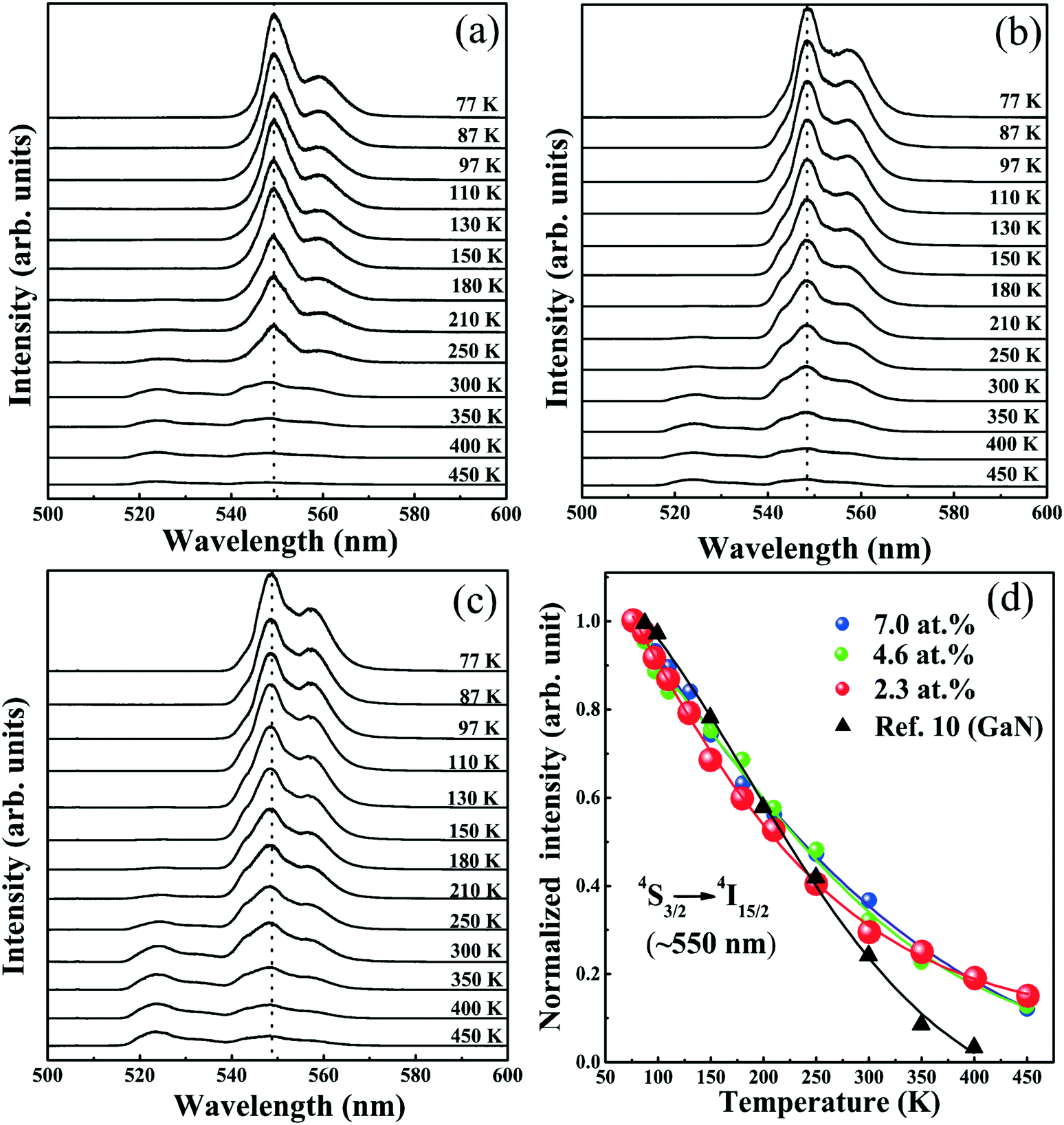 | ||
| Fig. 5 Temperature-dependent PL spectra in the range from 77 to 450 K of (a) 2.3, (b) 4.6, and (c) 7.0 at% Er-doped Ga2O3 films. (d) Dependence of the normalized intensity of the 4S3/2 to 4I15/2 (550 nm) emission on temperature.15 | ||
3. LEDs based on Ga2O3:Er/Si heterojunctions
Since sapphire is not conductive, it is not possible to fabricate optical devices operating between the films and the substrates. Moreover, Ga2O3:Er/Si heterojunctions are especially attractive due to the well-known advantage of the Si substrate and their prominent application in Si-based optoelectronic integrated circuits.26,27 Herein, the deposited Er-doped Ga2O3 film on a Si substrate was characterized using XPS to illustrate the chemical composition and chemical state. From Fig. 6(a), it is clear that two symmetrical peaks of Ga 2p1/2 and Ga 2p3/2 are located at 1146 eV and 1119 eV, respectively. The separation energy between these two peaks is about 27 eV, which is in good agreement with the reported value for the Ga2O3 bulk.28 Since the surface of the film was etched, the O 1s peak at 532 eV could be assigned to oxygen in the Ga2O3 lattice, as shown in Fig. 6(b). Fig. 6(c) reveals the XPS spectrum of the Er 4p core level and exhibits a peak centered at 321 eV. The Er content in the Ga2O3 film has been found to be 2.7 at% from the XPS spectra after applying an atomic sensitivity factor, which is almost the same as that of the target. These results confirm that Er atoms have been effectively incorporated into the oxide matrix.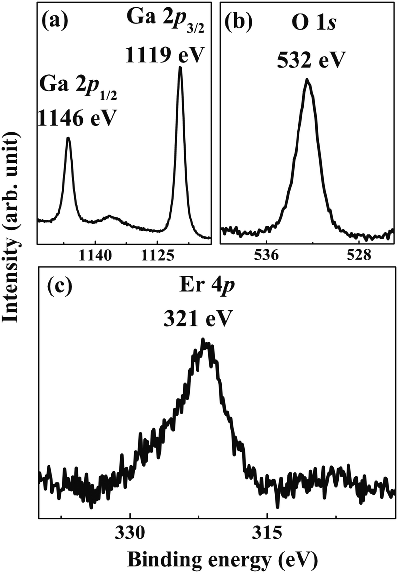 | ||
| Fig. 6 XPS spectra of (a) Ga 2p1/2, Ga 2p3/2, (b) O 1s, and (c) Er 4p core level for Er-doped Ga2O3 film.16 | ||
Fig. 7 shows the XRD pattern of the Er-doped Ga2O3 film. In addition to the substrate diffraction peaks at 28° and 59°, two peaks can be clearly observed at 31° and 45°, which can be assigned to the (−401) and (−601) planes of Ga2O3, respectively.
 | ||
| Fig. 7 XRD patterns of the Ga2O3 film on the Si substrate.17 | ||
Fig. 8 shows the schematic of the Ga2O3:Er/Si LEDs. To form electrical contacts, ∼200 nm thick indium tin oxide layer was deposited onto the Er-doped Ga2O3 film by direct current sputtering. Herein, ∼250 nm Au films were formed on the backside of the Si substrate using an electron beam evaporated technique. The current–voltage (I–V) characteristics of the EL spectra were measured by an Advantest DC voltage current source (R6364), and the EL spectra were obtained in the visible region using a high sensitivity spectra multichannel photo detector (MCPD-7000).
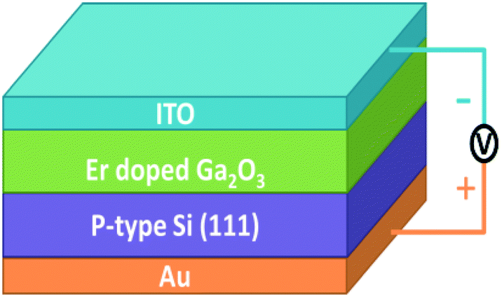 | ||
| Fig. 8 Schematic of the Ga2O3:Er/Si LEDs. | ||
Fig. 9 shows the I–V characteristic of the Ga2O3:Er/Si LEDs. Note that an excellent rectification character was obtained, indicating that the devices were a p–n heterojunction. Herein, the devices were electroluminescent only under the forward bias; this demonstrated that the simultaneous injection of electrons and holes was necessary for EL.29 Strikingly, the current rapidly increases when the forward bias voltage is above 6.2 V, and it is strongly blocked under the reverse bias. It was validated that green emission originated from Er ions incorporated into Ga2O3 could be activated with a voltage as low as 6.2 V. From the inset of Fig. 9, a leakage current of 2.0 mA can be determined at −6.2 V, whereas the current reaches 60 mA at 6.2 V. Moreover, note that the bright green emission can be observed by the naked eye at the forward bias of 6.2 V.
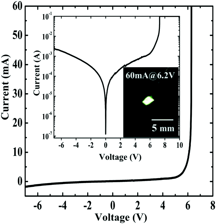 | ||
| Fig. 9 The I–V characteristic of the Ga2O3:Er/Si LEDs. Inset shows the same characteristic with log scale and the EL image of this device in dark at 60 mA.16 | ||
To investigate the origin of EL emission of Er ions, the PL spectrum of Er-doped Ga2O3 films excited by 488 nm light is shown in Fig. 10(a). The strongest green emission band centered at 548 nm can be observed in the PL spectrum, which is caused by the 4S3/2 to 4I15/2 transition. Other PL peaks observed at 524, 660, 850, and 975 nm can be assigned to the transitions from 2H11/2 to 4I15/2, 4F9/2 to 4I15/2, 4I9/2 to 4I15/2, and 4I11/2 to 4I15/2, respectively.3,15 We have deconvoluted the green emission bands in this spectrum with four Gaussian curves at the wavelengths positioned at 524, 533, 548, and 559 nm. Herein, two weak peaks at 533 and 559 nm were ascribed to Stark splitting due to the spin–orbit splitting of the energy level.18Fig. 10(b) shows the EL spectra of the fabricated Ga2O3:Er/Si LEDs under different forward bias voltages. It is clear that the EL intensity increases with the forward bias, and no peak shift in the EL spectrum is observed with the injection current ranging from 3 to 60 mA. Moreover, the EL spectra has two narrow, strong green emission bands centered at 524 and 548 nm, which are consistent with the PL results.
 | ||
| Fig. 10 (a) Room temperature (RT) PL spectrum of Er-doped Ga2O3 films. (b) RT-EL spectra for the Ga2O3:Er/Si LEDs with different current injections.16 | ||
Fig. 11(a) shows the plots of the EL intensity of green emission at 524 and 548 nm with forward bias voltage. The EL intensity of 548 nm becomes consistently stronger than that of the 524 nm emission with the increasing injection current. The most likely explanation is that the intensity from the upper 2H11/2 (524 nm) level is reduced as it increasingly feeds electrons to the lower 4S3/2 (548 nm) level due to two closely spaced electronic states.3 Note that the EL intensity rapidly increases when the forward bias voltage is above 6.2 V, which confirms that the driven voltage for the onset green emission is ∼6.2 V. In Fig. 11(b), we present the light intensity of green emissions at 524 and 548 nm and the injection current (L–I) characteristics of this device. In agreement with the spectral evolution, the results can be fitted by the power law:
| L ∼ Im |
 | ||
| Fig. 11 (a) Forward bias voltage dependence of the EL intensities of the Ga2O3:Er/Si LEDs. (b) EL intensity as a function of the injection current for the green emission at 524 and 548 nm.16 | ||
4. Band offset of the Ga2O3/Si heterojunction interface
As is known, band offset is one of the most important electronic parameters of the semiconductor heterojunction because it determines the energy barriers for electron and hole transport that are essential for the operation of the devices. The valence band offset (VBO) (ΔEv) of the Ga2O3/Si heterojunction can be calculated using Kraut's method.33,34 In this study, we used a thick Ga2O3 film (550 nm) as the bulk-like sample. First, we determined the valence band maxima (VBM) energies and core levels (CLs) positions for the thick Ga2O3 film and Si substrate. Fig. 12(a) and (b) show Si 2p CL and the valence band for Si substrate. Using the fitting methods described in the experimental section, it was found that the binding energy for Si 2p was located at 100.2 eV. The VBM is determined to be 0.3 eV. Similar values for the Si substrate have been obtained by You et al.29Fig. 12(c) and (d) reveal Ga 2p3/2 CL and valence band of the thick Ga2O3 film, respectively. Using the same method as that use for the Si substrate, the binding energy for Ga 2p3/2 has been found to be 1119.4 eV, whereas the VBM value has been determined to be 3.7 eV. As reported in the literature, Jia et al.35 have investigated the VBM value of Ga2O3 to be 3.69 eV, which is consistent with the value determined in this study.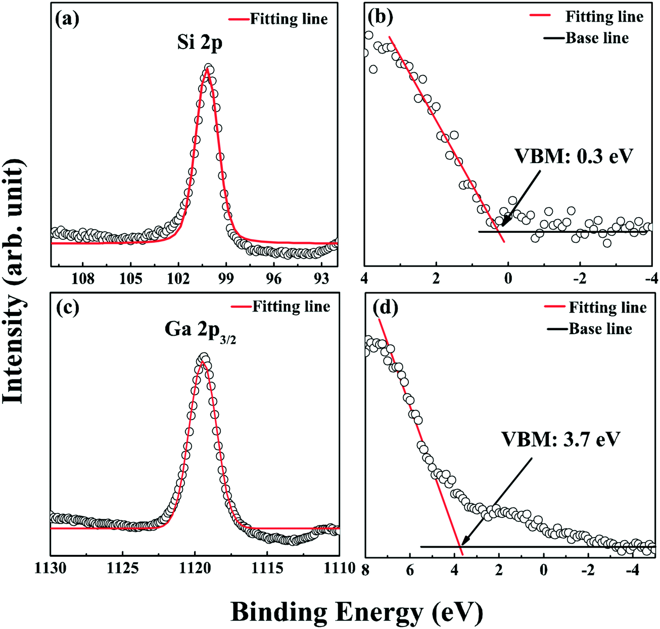 | ||
| Fig. 12 (a) Si 2p CL spectrum and (b) valence band spectrum for the Si substrate. (c) Ga 2p3/2 core level spectrum and (d) valence band spectrum for the 550 nm thick Ga2O3 film.17 | ||
We have reported that the measurements for CL separation of the Ga2O3/Si interface are very important to ensure the veracity of the measured VBO value. Moreover, the overlayer of a heterojunction must be sufficiently thin to allow CLs from the underlying material to be probed due to the finite escape depth of the photoelectron.36 Therefore, we fabricated the interface of Ga2O3/Si by etching a 30 nm thick film by repeating Ar+ ion sputtering until both Ga 2p3/2 and Si 2p photoelectron peaks were observed in the spectra. Fig. 13 shows a series of Ga 2p3/2, Ga 3p1/2, Ga 3p3/2, and Si 2p photoemission spectra observed from (a) Ga2O3 thick film, (b) Ga2O3/Si interface, and (c) near Si substrate. We found that the Si 2p peak appeared and its intensity increased with the increasing Ar+ ion sputtering time. Conversely, the intensity of the Ga 2p3/2, Ga 3p1/2, and Ga 3p3/2 peaks decreased with the increasing sputtering time. From Fig. 13(c), it can be observed that the CL spectrum of Ga 2p3/2 peak consists of two components: one is attributed to the Ga–O bond, whereas the other may be attributed to the Ga–Ga bond in the initial stages of growth of the film on the Si substrate.37 Herein, it is worth noting that whether an ultrathin SiOx layer is formed at the Ga2O3/Si interface during the growth of the Ga2O3 film. In this study, the peaks corresponding to the Si–O bond were not observed at the Ga2O3/Si interface, as shown in Fig. 13(b); this indicated that the effect of interfacial state as well as the ultrathin SiOx layer should be neglected.29,38,39 We calculated the VBO value of the Ga2O3/Si heterojunction to be 3.5 eV. On the other hand, the conduction band offset (CBO) can be determined to be 0.2 eV; this means that the conduction band level of Si is lower than that of Ga2O3. In the literature, Guo et al.40 have calculated the VBO and CBO values of the Ga2O3/Si structure to be 2.63 and 1.10 eV, respectively. These values are substantially different from the experimental data obtained in this study. When a voltage bias is applied on the Ga2O3/Si heterojunction, the electrons flow from the conduction band of Ga2O3 to the Si conduction band, and the holes can be injected from the valence band of Si to that of Ga2O3 under a certain bias.39,41 Based on these results, a type I schematic band alignment of the Ga2O3/Si heterojunctions is shown in Fig. 14(a). As shown in Fig. 14(b), when a forward bias is applied on the heterojunction, a number of electrons in the ITO electrode can be thermally activated to tunnel into the trap states near the interface.42 The electrons flow from the conduction band of Ga2O3 to that of Si. The holes can be injected from the valance band of the Si substrate to that of Ga2O3 under a certain bias, despite the possibility that the device may be electron flow dominated.39 In this context, under the aforementioned forward bias voltage, a part of electrons in the conduction band of Ga2O3 will directly recombine with the holes in the valence band. However, since Ga2O3 is a direct bandgap semiconductor,43,44 transfer of energy released from the direct electron–hole recombination to Er ions is negligible due to the short lifetime.8 On the other hand, other electrons will first transit to the defect-related energy levels (EDefect) and then recombine with holes in the valance band of Ga2O3. The indirect recombination of carriers in the Ga2O3 host could transfer energy to the incorporated Er3+ ions near the defects. Similar energy transfer mechanisms have been demonstrated in ZnO:Er/Si devices.8 Heikenfeld et al.45 observed a driven voltage of ∼8.5 V when the thickness of the GaN:Er layer was 600 nm. Zavada et al.6 reported Er-doped III-N diodes that exhibited green luminescence under the forward bias voltage ranging from 10 to 15 V. Harako et al.7 have demonstrated green EL from ZnO:Er/Si diodes with a driven voltage of ∼10 V. Based on the abovementioned experimental results, it is obvious that the driven voltage of green emission from Ga2O3:Er/Si LEDs in this study is lower than that of ZnO:Er/Si and GaN:Er/Si devices. It has been demonstrated that the wide bandgap of Ga2O3 contains more defect-related levels.46–48 Thus, we believe that the low driven voltage from Ga2O3:Er/Si LEDs is ascribed to the wide bandgap of Ga2O3 that will enhance the effects of radiative recombination between electrons in the defect-related level and holes in the valence band; this would result in the improvement of energy transfer.47
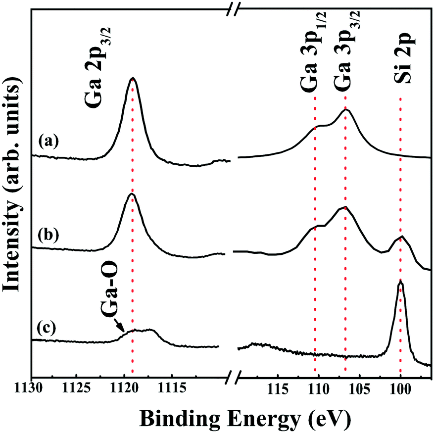 | ||
| Fig. 13 Ga 2p3/2, Ga 3p1/2, Ga 3p3/2, and As 3d core levels spectra observed from (a) the Ga2O3 thick film, (b) Ga2O3/Si interface, and (c) near Si substrate obtained by changing the Ar+ ion sputtering time.17 | ||
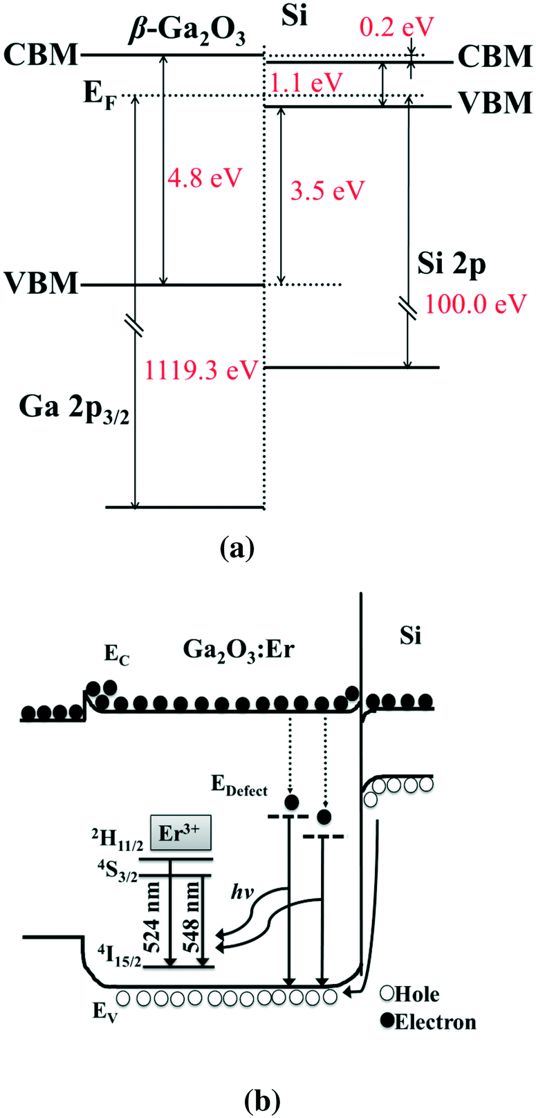 | ||
| Fig. 14 Schematic for the energy band structure and transfer energy process of the Ga2O3:Er/Si LEDs (a) at thermal equilibrium and (b) under forward bias.16,17 | ||
5. Summary
We have briefly reviewed the effect of the doping content on the structure, surface morphology, and optical properties of the Er-doped Ga2O3 films on sapphire and Si substrates. Pure green luminescence at 550 nm has been observed from all the samples. LEDs based on the Ga2O3:Er/Si heterojunctions have been successfully fabricated. Bright pure green emission can be observed by the naked eye from the LEDs. Moreover, the wide bandgap of Ga2O3 contains more defect-related levels, which will enhance the effects of recombination between electrons in the defect-related level and the holes in the valence band, thus resulting in the improvement of energy transfer to Er ions. The driven voltage of this LED is 6.2 V, which is lower than those of ZnO:Er/Si and GaN:Er/Si devices. To analyze the transfer energy process, we also investigated the band offsets of the Ga2O3/Si heterojunction interface. The valence band offset and conduction band offset have been determined to be 3.5 eV and 0.2 eV, respectively.Acknowledgements
This work was partially supported by the Scientific Research (No. 16K06268) and the Partnership Project for Fundamental Technology Researches of the Ministry of Education, Culture, Sports, Science and Technology, Japan.References
- M. Garter, J. Scofield, R. Birkhahn and A. J. Steckl, Appl. Phys. Lett., 1999, 74, 182–184 CrossRef CAS
.
- S. Nakamura, T. Mukai and M. Senoh, J. Appl. Phys., 1994, 76, 8189–8191 CrossRef CAS
- A. J. Steckl and R. Birkhahn, Appl. Phys. Lett., 1998, 73, 1700–1702 CrossRef CAS
- H. Q. Wu, C. B. Poitras, M. Lipson, M. G. Spencer, J. Hunting and F. J. DiSalvo, Appl. Phys. Lett., 2005, 86, 191918 CrossRef
- R. Birkhahn and A. J. Steckl, Appl. Phys. Lett., 1998, 73, 2143–2145 CrossRef CAS
- J. M. Zavada, S. X. Lin, N. Nepal, J. Y. Lin, H. X. Jiang, P. Chow and B. Hertog, Appl. Phys. Lett., 2004, 84, 1061–1063 CrossRef CAS
- S. Harako, S. Yokoyama, K. Ide, X. Zhao and S. Komoro, Phys. Status Solidi A, 2008, 205, 19–22 CrossRef CAS
- Y. Yang, Y. P. Li, L. L. Xiang, X. Y. Ma and D. R. Yang, Appl. Phys. Lett., 2013, 102, 181111 CrossRef
- P. N. Favennec, H. L'Haridon, M. Salvi, D. Moutonnet and Y. L. Guillou, Electron. Lett., 1989, 25, 718–719 CrossRef
- A. J. Steckl, M. Garter, R. Birkhahn and J. Scofield, Appl. Phys. Lett., 1998, 73, 2450–2452 CrossRef CAS
- X. Wang, Z. W. Chen, F. B. Zhang, K. Saito, T. Tanaka, M. Nishio and Q. X. Guo, Ceram. Int., 2016, 42, 12783–12788 CrossRef CAS
- Z. W. Chen, K. Saito, T. Tananka, M. Nishio, M. Arita and Q. X. Guo, J. Cryst. Growth, 2015, 430, 28–33 CrossRef CAS
- F. B. Zhang, K. Saito, T. Tanaka, M. Nishio and Q. X. Guo, J. Cryst. Growth, 2014, 387, 96–100 CrossRef CAS
- Z. W. Chen, X. Wang, F. B. Zhang, S. Noda, K. Saito, T. Tanaka, M. Nishio and Q. X. Guo, J. Lumin., 2016, 177, 48–53 CrossRef CAS
- Z. W. Chen, X. Wang, S. Noda, K. Saito, T. Tanaka, M. Nishio, M. Airita and Q. X. Guo, Superlattices Microstruct., 2016, 90, 207–214 CrossRef CAS
- Z. W. Chen, X. Wang, F. B. Zhang, S. Noda, K. Saito, T. Tanaka, M. Nishio, M. Arita and Q. X. Guo, Appl. Phys. Lett., 2016, 109, 022107 CrossRef
- Z. W. Chen, K. Nishihagi, X. Wang, K. Saito, T. Tanaka, M. Nishio, M. Arita and Q. X. Guo, Appl. Phys. Lett., 2016, 109, 102106 CrossRef
- P. Gollakota, A. Dhawan, P. Wellenius, L. M. Lunardi, J. F. Muth, Y. N. Saripalli, H. Y. Peng and H. O. Everitt, Appl. Phys. Lett., 2006, 88, 221906 CrossRef
- Z. P. Wu, G. X. Bai, Q. R. Hu, D. Y. Guo, C. L. Sun, L. Y. Ji, M. Lei, L. H. Li, P. G. Li, J. H. Hao and W. H. Tang, Appl. Phys. Lett., 2015, 79, 171910 CrossRef
- D. H. A. Blank, M. E. Bijlsma, R. Moerman, H. Rogalla, F. J. B. Stork and A. Roshko, J. Alloys Compd., 1997, 251, 31–33 CrossRef CAS
- E. Nogales, J. A. García, B. Méndez, J. Piqueras, K. Lorenz and E. Alves, J. Phys. D: Appl. Phys., 2008, 41, 065406 CrossRef
- Y. Jia, K. Zeng, J. Wallace, J. Gardella and U. Singisetti, Appl. Phys. Lett., 2015, 106, 102107 CrossRef
- A. J. Neuhalfen and B. W. Wessels, Appl. Phys. Lett., 1991, 59, 2317–2319 CrossRef CAS
- S. Q. Chen, B. Dierre, W. Lee, T. Sekiguchi and S. Tomita,
et al.
, Appl. Phys. Lett., 2010, 96, 181901 CrossRef
- X. Z. Wang and B. W. Wessels, Appl. Phys. Lett., 1994, 64, 1537–1539 CrossRef CAS
- X. P. Li, B. L. Zhang, X. Dong, Y. T. Zhang, X. C. Xia, W. Zhao and G. T. Du, J. Lumin., 2009, 129, 86–89 CrossRef CAS
- P. L. Chen, X. Y. Ma and D. R. Yang, J. Appl. Phys., 2007, 101, 053103 CrossRef
- G. Schön, J. Electron Spectrosc. Relat. Phenom., 1973, 2, 75–86 CrossRef
- J. B. You, X. W. Zhang, S. G. Zhang, H. R. Tan, J. Ying, Z. G. Yin, Q. S. Zhu and P. K. Chu, J. Appl. Phys., 2010, 107, 083701 CrossRef
- J. D. Ye, S. L. Gu, S. M. Zhu, W. Liu, S. M. Liu, R. Zhang, Y. Shi and Y. D. Zheng, Appl. Phys. Lett., 2006, 88, 182112 CrossRef
- Y. I. Alivov, J. E. V. Nostrand, D. C. Look, M. V. Chukichev and B. M. Ataev, Appl. Phys. Lett., 2003, 83, 2943–2945 CrossRef CAS
- M. Ishii, A. Koizumi, Y. Takeda and Y. Fujiwara, J. Appl. Phys., 2014, 115, 133510 CrossRef
- S. D. Singh, R. S. Ajimsha, V. Sahu, R. Kumar, P. Misra, D. M. Phase, S. M. Oak, L. M. Kukreja, T. Ganguli and S. K. Deb, Appl. Phys. Lett., 2012, 101, 212109 CrossRef
- V. Thakur and S. M. Shivaprasad, Appl. Surf. Sci., 2015, 327, 389–393 CrossRef CAS
- Y. Jia, K. Zeng, J. Wallace, J. Gardella and U. Singisetti, Appl. Phys. Lett., 2015, 106, 102107 CrossRef
- Q. X. Guo, K. Takahashi, K. Saito, H. Akiyama, T. Tanaka and M. Nishio, Appl. Phys. Lett., 2013, 102, 092107 CrossRef
- V. Thakur and S. M. Shivaprasad, Appl. Surf. Sci., 2015, 327, 389–393 CrossRef CAS
- X. P. Li, B. L. Zhang, X. Dong, Y. T. Zhang, X. C. Xia, W. Zhao and G. T. Du, J. Lumin., 2009, 129, 86–89 CrossRef CAS
- J. Robertson and B. Falabretti, J. Appl. Phys., 2006, 100, 014111 CrossRef
- X. C. Guo, N. H. Hao, D. Y. Guo, Z. P. Wu, Y. H. An, X. L. Chu, L. H. Li, P. G. Li, M. Lei and W. H. Tang, J. Alloys Compd., 2016, 660, 136–140 CrossRef CAS
- Z. Z. Yuan, D. S. Li, M. H. Wang, P. L. Chen, D. R. Gong, P. H. Cheng and D. R. Yang, Appl. Phys. Lett., 2008, 92, 121908 CrossRef
- B. He, Z. Q. Ma, J. Xu, L. Zhao, N. S. Zhang, F. Li, C. Shen, L. Shen, X. J. Meng, C. Y. Zhou, Z. S. Yu and Y. T. Yin, Superlattices Microstruct., 2009, 46, 664–671 CrossRef CAS
- J. B. Varley, J. R. Weber, A. Janotti and C. G. Van de Walle, Appl. Phys. Lett., 2010, 97, 142106 CrossRef
- F. B. Zhang, K. Saito, T. Tanaka, M. Nishio and Q. X. Guo, Solid State Commun., 2014, 186, 28–31 CrossRef CAS
- J. Heikenfeld, D. S. Lee, M. Garter, R. Birkhahn and A. J. Steckl, Appl. Phys. Lett., 2000, 76, 1365–1367 CrossRef CAS
- L. Binet and D. Gourier, Appl. Phys. Lett., 2000, 77, 1138–1140 CrossRef CAS
- K. Irmscher, Z. Galazka, M. Pietsch, R. Uecker and R. Fornari, J. Appl. Phys., 2011, 110, 063720 CrossRef
- Z. Zhang, E. Farzana, A. R. Arehart and S. A. Ringel, Appl. Phys. Lett., 2016, 108, 052105 CrossRef
| This journal is © The Royal Society of Chemistry 2017 |