
Crystal engineering for novel functionalities with oxide thin film epitaxy
Daichi
Oka
a and
Tomoteru
Fukumura
*ab
aDepartment of Chemistry, Graduate School of Science, Tohoku University, Sendai 980-8578, Japan. E-mail: tomoteru.fukumura.e4@tohoku.ac.jp
bWPI Advanced Institute for Materials Research, Tohoku University, Sendai 980-8577, Japan
First published on 6th March 2017
Abstract
Oxides have become recognized as one of the most promising next-generation electronic materials due to the varieties of rich functionalities such as superconductivity, ferromagnetism, ferroelectricity, transparency, etc. In addition to the great diversity of functionalities, oxygen affinity with many other elements provides opportunities for crystal engineering in oxides: the properties can be tuned by modification of the bonding state of oxide ions. Epitaxy has been used as a powerful method to conduct such crystal engineering on oxides in the form of thin films. We give a review of recent advancements related with crystal engineering of oxide thin films via epitaxy techniques that control the microscopic crystallographic environment.
1 Introduction
Over the long period of human history, oxides have been used as structural materials, insulators, and ceramics because of their superior stability in air. In this half century, their versatile functionalities have been unveiled, such as transparency, electric/ionic conductivity, ferroelectricity, ferromagnetism, multiferroicity, and superconductivity, all of which could contribute to key functions in next generation devices.1–8 In contrast with established semiconductors such as Si and III–V compounds, oxides possess a large number of chemical compositions and crystal structures owing to the extraordinary affinity of oxygen to many elements. The oxygen affinity also enables the formation of various kinds of atomic coordination networks via oxygen ions, providing the possibility of combining various functionalities and constructing future devices beyond silicon-based technology.9 Accordingly, “crystal-engineering” is useful to control properties of oxides by changing the microscopic crystallographic environment as described in this article.In the initial period of oxide electronics, oxides have been investigated as ceramic materials mainly in the form of bulk powders, sintered pellets, and polycrystalline films on demand of the traditional ceramic industry. Such oxides are usually the most stable phases due to the mostly thermodynamic equilibrium processes. Since the discovery of high-Tc superconductivity in layered cuprates,10 the significant progress of thin film epitaxy techniques of oxides has boosted oxide electronics. For example, high quality epitaxial thin films are indispensable for the fabrication of heteroepitaxial structures such as the Josephson junction.11 In addition, such epitaxy techniques are useful not only for thin film growth of existing functional oxides but also for thin film synthesis of new compounds and metastable phases via crystal engineering of oxides.12–14
At the initial stage of epitaxial growth, a single crystalline substrate serves as a seed for thin film crystallization. The initially deposited thin film becomes a self-seed for the subsequently deposited thin film, and eventually a complete epitaxial thin film is deposited. Single crystalline substrates stabilize various metastable structures owing to the epitaxial force, yielding novel functionalities. Such behaviour has already been recognized in the cases of Si and III–V semiconductors. However, more ionic oxides seem to be more attractive to tailor various structures and functionalities via crystal engineering using thin film epitaxy.
In this review article, we provide an overview of the recent progress in thin film epitaxy of homogeneously structured oxides as a convenient tool to create rich functionalities through chemical design. In section 2, representative film growth techniques are introduced. In section 3, successful examples of crystal engineering of oxides are described, as schematically shown in Fig. 1. This review article does not intend to cover all fields and pioneering works of oxide epitaxial thin films. A detailed insight into the heteroepitaxy of nonisostructural complex oxides has been recently reviewed by Wong et al.15 Extensively studied oxide heterointerfaces, heterostructures, and self-assembled structures are discussed elsewhere.16–19
 | ||
| Fig. 1 Schematic diagram of a perovskite heterostructure with compressive strain showing the possible influence of epitaxy on thin films. | ||
2 Film growth techniques
Various techniques of oxide thin film epitaxy have been developed so far (Table 1). Pulsed laser deposition (PLD), sputtering deposition, and molecular beam epitaxy (MBE) are classified as physical vapour deposition methods, in which atomic, molecular, and/or ionic chemical species are physically evaporated by means of laser irradiation, ion bombardment, and thermal heating, respectively. These highly established and easy-to-use techniques are widely used because of the availability of high quality thin films. On the other hand, chemical vapour deposition (CVD) and some solution-based methods are cost-effective and easy-to-modify processes. Also, novel deposition techniques such as hybrid MBE, atomic layer deposition (ALD), and mist CVD have been developed for scientific and industrial studies.| Methods | Sources | Supply | Atmosphere | Pressure (Pa) | Particle energy (eV) | Temperature (°C) | Advantage | Disadvantage |
|---|---|---|---|---|---|---|---|---|
| Pulsed laser deposition | Sintered ceramics/single crystals | Laser ablation | Vacuum, O2, Ar, H2, N2, or mixtures | OP: BP–10 | 1–100 | 500–1200 | • Stoichiometric transfer • Wide applicability | • Low growth rate • Spontaneous defect formation |
| BP: 10−7–10−6 | ||||||||
| Sputtering | Sintered ceramics/metal plates | Sputtering | Ar, Ne, Kr, Xe, O2, H2, N2 or mixtures | OP: 10−2–10 | 1–10 | 500–800 | • High growth rate • Large area | • Damage by ionized particle • Elemental selective supply rate |
| BP: 10−6–10−3 | ||||||||
| Molecular beam epitaxy | Elemental substances/metal organics | Thermal evaporation | Vacuum, O2, or O3 | OP: BP–10−5 | 0.1–1 | 500–1200 | • Easy control of supply ratio of elements • Precise stoichiometry (hybrid MBE) | • Low growth rate • Fixed target |
| BP: 10−8–10−7 | ||||||||
| Chemical vapour deposition | Metal organics/hydride/halide | Thermal evaporation and gas flow | H2, N2, O2, O3, H2O or mixtures | 100–AP | 0.1–1 | 100–800 | • Easy control of composition | • Low crystallinity • Limitation of precursor (vapour pressure) |
| Atomic layer deposition | Metal organics | Thermal evaporation of precursor molecules | O2, O3, N2 | 100–AP | 0.1–1 | 200–400 | • Flat even on textured surface • Large area | • Fixed target |
| Solution route | Precursors soluble in solvents | Direct supply of precursor solutions | Atmospheric or controlled conditions | AP | — | 500–1000 | • Easy setup • Large area | • Low crystallinity |
| Mist chemical vapour deposition | Precursors soluble in solvents | Gas flow of precursor solution mist | O2, O3, N2 | AP | — | 500–1000 | • Easy setup • Large area | • Limitation of pressure |
| Solid phase epitaxy | — | — | Atmospheric or controlled conditions | 10−7–AP | — | 500–1200 | • Flexible control of conditions | • Highly material dependent |
Growth mechanism and phase stability depend on each technique. In gaseous phase processes, the oxidation state of the thin film can be tuned by proper supply of gases such as oxygen and ozone. In solution processes, the oxidation state can be tuned by oxidizers and reductants. The kinetic energy of the deposited species is an important factor.20 The kinetic energy in the case of thermal evaporation techniques such as MBE and CVD is as small as ∼0.1 eV, often resulting in formation of the most stable phase with less intrinsic chemical vacancies in crystals. In contrast, sputtering deposition and PLD generate species with a high kinetic energy of several eV for the deposition of oxides. The deposited species such as atoms and molecular clusters are sometimes trapped at a local minimum state in the energy landscape rather than the global minimum state owing to the high kinetic energy; thus metastable phases are sometimes formed. Also in the case of low temperature thermal processes such as ALD and topotactic reactions, metastable phases are sometimes obtained because of the reaction not attaining the global minimum. In this section, the basic principles of film synthetic methods and recent advances are described from the viewpoint of crystal engineering.
2.1 Pulsed laser deposition
The main components of PLD are a precursor target and a substrate usually placed face-to-face with each other in a vacuum chamber and a high power laser for ablation of the target (Fig. 2a).21,22 The target is typically a sintered ceramic pellet or a single crystal of oxides, and its composition is the same as that of the films because of usually unchanged transfer of the composition during deposition as described below. A short wavelength is generally preferable in the case of oxides because negligible particles are generated on the film due to the short penetration depth of laser light. The most commonly used lasers are the Nd:Y3Al5O12 (Nd:YAG) solid state laser with a harmonic wavelength λ between 255 and 1064 nm and ultraviolet excimer gas lasers such as KrF (λ = 248 nm), XeCl (λ = 308 nm), and ArF (λ = 157 nm). Excimer lasers possess higher energy stability in the ultraviolet region, and hence are appropriate to deposit flat and dense films of oxides. The atmospheric conditions inside the chamber are highly flexible depending on the film compounds: various gases such as O2, N2, H2, Ar, NO2, etc. can be used at a wide range of pressures from 0 to ∼100 Pa. The ablation process with a nanosecond scale duration, ∼5 ns and ∼20 ns for Nd:YAG and excimer lasers, respectively, consists of complicated multiple steps despite a seemingly simple process.23 When a target is ablated by a laser pulse, the target surface is locally heated up rapidly within the picosecond scale to melt and then evaporate. The ejecta, so-called plume, absorbs the laser pulse to promote plasma formation including electrons, ions, molecular clusters, and so on. Subsequently, the adiabatically expanded plume is propagated normal to the target surface on the substrate, resulting in film deposition. The directional and instantaneous propagation of the plume contributes to an approximately complete transfer of the chemical composition from the target to the film, which is a considerable advantage of PLD. This is the case especially when the atmosphere is under high vacuum, in which collision between the ejected species and the existing gaseous molecules is negligible24 though the transfer of stoichiometric composition is not always ideal as described in section 3. Because of the high kinetic energy of the chemical species in plume under high vacuum, the PLD process is highly non-equilibrium, sometimes leading to the formation of metastable phases.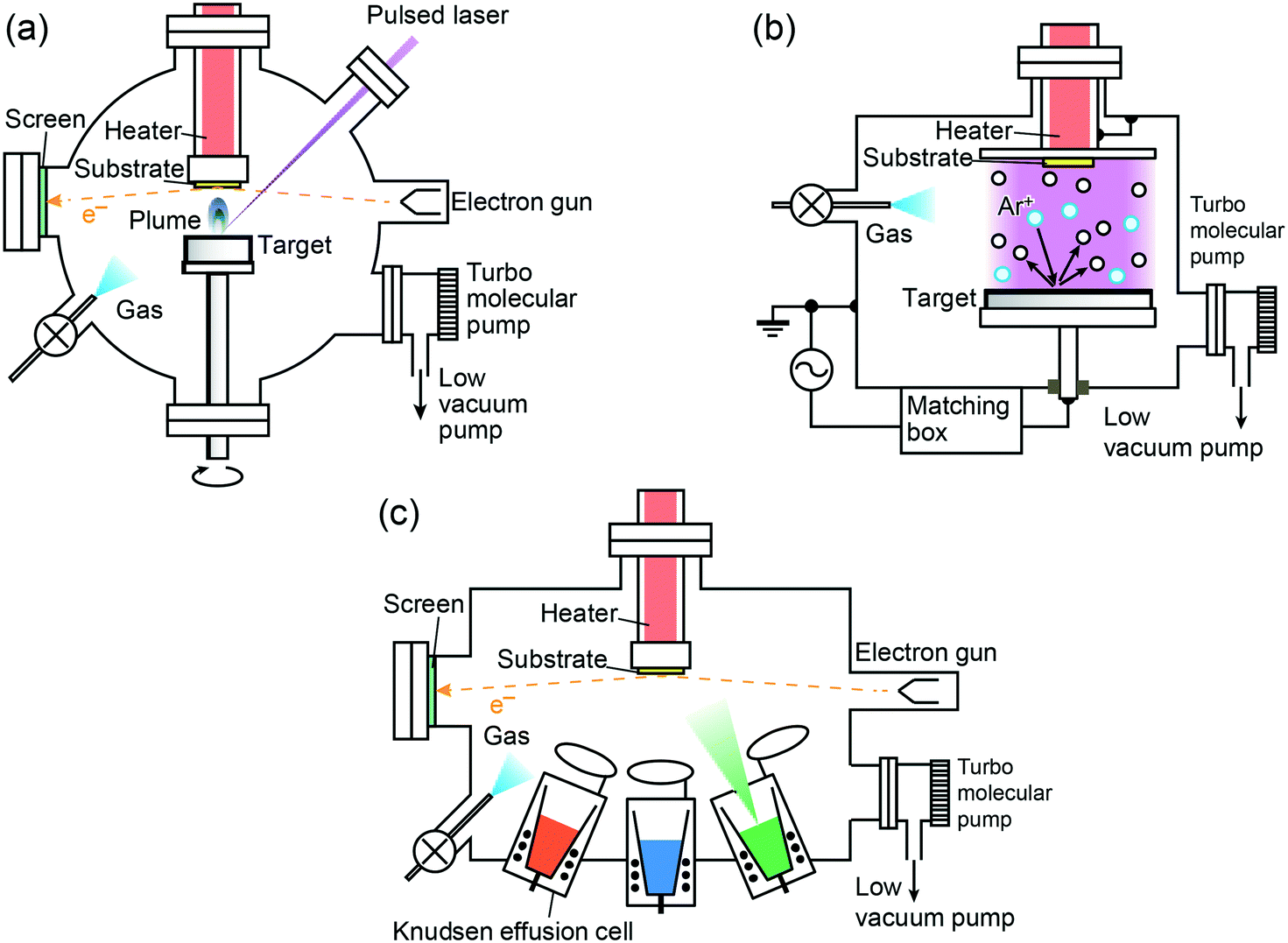 | ||
| Fig. 2 Typical setups of physical vapour deposition. (a) Pulsed laser deposition, (b) rf sputtering deposition, and (c) molecular beam epitaxy. | ||
PLD chambers are generally equipped with a substrate heater for high temperature deposition. A halogen lamp surrounded by a gold mirror has been widely used for the heater. Today, infrared continuous solid state lasers such as the Nd:YAG laser, which was originally used as a steel cutter, are available for higher temperature and rapid heating and cooling.25 The substrate temperature quickly exceeds over 1000 °C. Also, reduction of the laser spot size is useful to make a temperature gradient within a 1 cm-sized substrate, enabling rapid optimization of growth temperature.26 Such efficient optimization of growth parameters was attempted also for film composition by using a combinatorial approach.27 Here, the system is equipped with a combination of automatic moving masks and a target exchanger, in which a combinatorial thin film library with discrete phases and composition-spread phases can be manufactured on a single substrate.
In situ monitoring of the film structure during growth is applied for efficient optimization of growth conditions and understanding of film growth mechanisms by using reflection high energy electron diffraction (RHEED). An electron beam arriving at the sample surface with a shallow incident angle is reflected and probed on a photoluminescence detector screen placed at the opposite side of the electron gun as a diffraction pattern (Fig. 2a). Because of the small penetration depth of the electron beam, the diffraction pattern reflects the crystal structure and morphology of the topmost surface of the film. The temporal change of diffraction intensity during deposition corresponds to the surface coverage and growth mode of molecular layers.28 Hence, the deposition of a superlattice can be conducted.29 By using the combinatorial approach, parallel synthesis of superlattices with different sequences is possible.30
2.2 Sputtering deposition
Sputtering deposition is one of the most frequently used film growth methods especially in industrial applications due to its large areal deposition with a high growth rate.31,32 The chamber is filled generally with inert gases such as noble gases and N2 with a pressure of around 1–10 Pa. For deposition of films, the electrical bias between an anode beneath the target and a cathode attached to the substrates accelerates positively ionized atoms of the process gas up to a kinetic energy of 0.1–10 keV, which impinge on the target surface on the anode, invoking a glow discharge with a relatively high current density.33 The ejected particles lose their kinetic energy significantly by collision with the high pressure gas molecules before reaching the substrate surface.For sputtering of insulators, high frequency rf voltage (typically 13.56 MHz) is applied, while dc voltage is used for conductors such as metals (Fig. 2b). Recently, magnetrons were often attached to the backside of targets for capturing secondary electrons from the target surface, in order to increase the yield rate of ejected atoms and to prevent sputtering damage of the film surface by the electrons. Reactive sputtering is also used to deposit oxide films by oxidizing metal species from the target under O2 gas during deposition, in which a dc voltage source is often used and is cost effective in spite of a lower deposition rate than that of rf sputtering.
A high kinetic energy of about 1 keV of incident ions required for a sufficient yield rate over unity (knock-on mode) tends to degrade film quality by generating defects such as grain boundaries and gas implantation. Hence, reduction of gas pressure has been attempted by several methods such as collimation of ions, gas ionization with rf induced plasma, and ion beam assisted deposition.34 Because of the different sputtering rate for each element and the multiple scattering of the ejected particles, stoichiometric transfer like the PLD process is usually difficult. Accordingly, binary oxides are the major target for the sputtering method, though precise optimization of deposition conditions enables the deposition of complex oxides and even their superlattices.35,36
2.3 Molecular beam epitaxy
MBE is a film growth method based on the straightforward concept of supplying each constituent atom of the objective material in an appropriate ratio. The constituent atoms are supplied on the substrate separately from Knudsen effusion cells under ultrahigh vacuum conditions (Fig. 2c).37 Oxygen is usually supplied from O2, O3, or O radical gases. Recently, a quite small MBE chamber, less than 1 m3 in volume, has been developed, enabling sample transfer in vacuo to vacuum measurement systems such as a synchrotron beam line,38 similar to a small PLD chamber.39Compared to PLD and sputtering, the MBE process supplies highly pure constituent elements with much smaller kinetic energy due to the thermal evaporation characteristics, usually realizing an almost thermal equilibrium condition. Thus, the resultant phase diagram is almost governed by thermodynamics.40,41 If the composition is properly tuned, highly stoichiometric and pure thin films of binary oxides can be deposited, as demonstrated by e.g. a fractional quantum Hall effect in the Mg0.05Zn0.95O/ZnO heterostructure.42
In the case of complex oxides, off-stoichiometry often happens because of a poorer desorption process due to the ionic nature of oxides. A breakthrough was achieved by the development of a technique called “hybrid MBE”, in which MBE and high vacuum CVD are combined.43 In this method organic metal is used as a precursor, which desorbs from the film in case of excess composition. Son et al. reported the highest electron mobility over 30![[thin space (1/6-em)]](https://www.rsc.org/images/entities/char_2009.gif) 000 cm2 V−1 s−1 in La-doped SrTiO3 epitaxial thin film deposited from Sr, La, oxygen plasma, and titanium tetraisopropoxide precursors.44 Matsubara et al. observed a quantum Hall effect in a δ-doped STO epitaxial thin film deposited using hybrid MBE.45 These results are indicative of the successful growth of ideally stoichiometric and very high quality films.
000 cm2 V−1 s−1 in La-doped SrTiO3 epitaxial thin film deposited from Sr, La, oxygen plasma, and titanium tetraisopropoxide precursors.44 Matsubara et al. observed a quantum Hall effect in a δ-doped STO epitaxial thin film deposited using hybrid MBE.45 These results are indicative of the successful growth of ideally stoichiometric and very high quality films.
2.4 Chemical vapour deposition
Chemical vapour deposition (CVD) using chemical reactions during deposition is categorized as a counterpart of physical vapour deposition techniques. CVD includes various relatives such as plasma CVD, low pressure CVD, and metal–organic CVD. These CVD processes are suitable for industrial applications because of high operation pressures from low vacuum to atmospheric pressure.CVD consists of three main processes: transfer of precursor molecules, chemical reactions at the substrate, and removal of by-products.31 Firstly, thermally evaporated precursors are transferred to the reactor by gas flow. Then, the precursors are in part adsorbed and decomposed into the objective solid phase and by-products on heated substrates in the reactor. The by-products, designed to have a higher vapour pressure, are desorbed from the substrate, yielding the objective material films. Compared to the homogeneous decomposition reaction of precursors in the gas phase prior to deposition on the substrate, the heterogeneous reaction of precursors on the substrate surface is preferable to deposit a dense and smooth film strongly bonded with the substrate.46 For the decomposition of precursors, plasma and light including laser can be used instead of heat, sometimes causing uncontrollable chemical reactions.47 Haga et al. succeeded in synthesizing high quality epitaxial thin films of ZnO by controlling the reactivity between Zn(C2H5)2 and CO2 with plasma.48 CVD processes under high vacuum conditions are also useful to synthesize unstable compounds under high pressure. In such processes, precursor species are supplied to the substrate as a molecular beam without collision like in MBE, and individual decomposition of each supplied molecule takes place.49 High vacuum CVD used for a Al2O3 film50 was later applied to high-TC superconductor thin films such as YBa2Cu3O7−x (ref. 51) and LaBa2Cu3O7−x.52 CVD combined with MBE was used for complex oxide thin films as described above.
2.5 Atomic layer deposition
ALD is an emerging technique to obtain highly flat and homogeneous films, categorized as a CVD process. Layer-by-layer self-limiting chemical reactions of organic precursors enable obtaining homogeneous films on various surfaces including nanostructures with a high aspect ratio.53,54 ALD can be conducted under low vacuum and low temperature, thus it is applied for various applications such as flat panel displays. For example, binary oxide AOx films are deposited in the following sequence (Fig. 3). Metal organic precursors supplied with inert gas are adsorbed on the bare substrate surface to form a single molecular layer with full coverage, and unreacted precursors and by-products are removed with inert gas by purging the chamber. Next, the layer was fully oxidized to form AOx by introducing co-reactants such as H2O and O3, followed by purging to remove redundant co-reactants and by-products. By repeating these cycles, a thin film of AOx is deposited in a layer-by-layer manner. For the deposition of complex oxides, the corresponding molecular layers are deposited alternately (e.g. AO and BO2 layers to form perovskite ABO3), resulting in difficult control of stoichiometry in ternary and quaternary oxides.55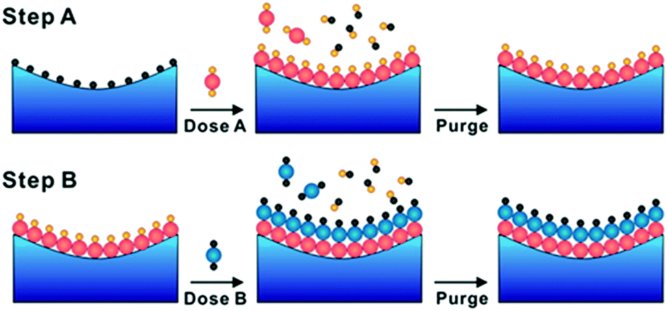 | ||
| Fig. 3 Depositing sequence of binary material using atomic layer deposition. Reproduced with permission from ref. 53. Copyright 2013, American Chemical Society. | ||
Recently, appropriate precursors were developed to obtain epitaxial thin films of ternary oxides. For example, Coll et al. reported the direct growth of spinel Co2FeO4 epitaxial thin films on the (100) and (110) planes of STO substrates at a low temperature of 250 °C.56 In this case, the Co-rich spinel pure phase was obtained as a fully relaxed film, exhibiting isotropic ferromagnetic behaviour down to 10 nm thick. Emery et al. reported the epitaxial growth of Sn doped In2O3 on the (100), (110), and (111) planes of YSZ substrate also at a low temperature of 250 °C.57 Excellent coherent growth on the substrate was seen in contrast with the case of the spinel films despite the lack of an atomically flat surface like MBE and PLD deposited films.
2.6 Solution process
One of the most frequently used solution processes in oxide film growth is the sol–gel method. In this method, precursor gels are prepared by dissolving metal compounds such as alkoxides into solvents, followed by hydrolysis and gelation reactions at a mild temperature of <100 °C.58 These gels are dip- or spin-cast on substrate homogeneously and are crystallized by calcination. During the gelation process, the component elements are homogeneously mixed at an atomic level in contrast to the vapour phase reactions, where the distribution of adsorbed atoms/molecules is predominated by kinetics, so that the film is formed almost in an equilibrium state. The easy processing is useful for practical applications, although there are several concerns such as the toxicity of organic solvents and precursors, insufficient growth rate, and poor film quality. Zhao et al. recently developed a fast growth route of YBa2Cu3O7−δ epitaxial thin films using a nontoxic propionate-based solution.59 The obtained film showed superconducting behaviour with a critical current density as high as 3.7 MA cm−2 at 77 K. Also, a technique called prompt inorganic condensation (PIC) is being studied extensively.60 In PIC, environmentally friendly aqueous solutions of metal nitrates are used as precursors in order to obtain high quality films.The solution process is suitable for complex oxides with multiplex crystallographic blocks due to its quasi-equilibrium nature. For example, Rivas-Murias et al. reported the successful synthesis of epitaxial thin films of misfit cobaltates ([AO]n[CoO2]) (A = Bi, Ba, Sr, Ca, Co) by sintering spin-coated aqueous solutions including polyethyleneimine.61 The polyethyleneimine decomposed at a slightly lower temperature than crystallization, preventing undesirable reactions, resulting in a clear epitaxial interface with LAO substrates. The cobaltates are composed of periodically stacked insulating rock salt [AO] layers and electrically conducting edge-sharing CoO6 octahedral layers, exhibiting bulk-like p-type electrical conduction and good thermoelectric properties. It is noted that epitaxial thin film deposition of the cobaltates was difficult by using physical vapour deposition techniques due to the interfacial amorphous layer probably formed by their non-equilibrium nature.62
2.7 Mist CVD
Mist CVD is a solution based technique developed recently (Fig. 4).63,64 A solution of precursors in a supply unit is converted into mist particles whose diameters are 2–3 μm using an ultrasonic transducer. The mist is diluted and transferred by carrier gas on the substrate in a reaction unit. Because of the simple setup operated under atmospheric pressure, the system is highly cost-effective. In addition, a high vapour pressure of precursors is unnecessary. The only requirement for precursors is solubility in solvents, which is not a difficult problem. | ||
| Fig. 4 Schematic setup of mist CVD. Reproduced with permission from ref. 63. Copyright 2014, The Japan Society of Applied Physics. | ||
The epitaxial growth of various binary oxides such as ZnO, Ga2O3, Al2O3 and In2O3 has been demonstrated.64 Despite the ambient growth conditions, these films showed high crystallinity with a narrow full width at half maximum (FWHM) of the rocking-curve, less than 0.01°, comparable to that of the vacuum processes.65 As a result, various thin films of mixed crystals and heterostructures have been deposited.64 Recent studies were extended to epitaxial thin film growth of ternary oxides such as bismuth iron and yttrium aluminium garnets.66,67
2.8 Topotactic reaction
A topotactic reaction is a post-deposition treatment to incorporate or remove elements while maintaining the crystal framework of mother compounds.68 Light ions with low electric charge such as H+, H−, Li+, O2− and F− are often used in topotactic reactions because of their high ionic conductivity. For topotactic reactions of oxides, gaseous, liquid, and solid reagents can be used. Though topotactic reactions can be conducted for both bulk and thin film specimens, the thin film specimen has an advantage due to the high speed and homogeneous reaction (Fig. 5).69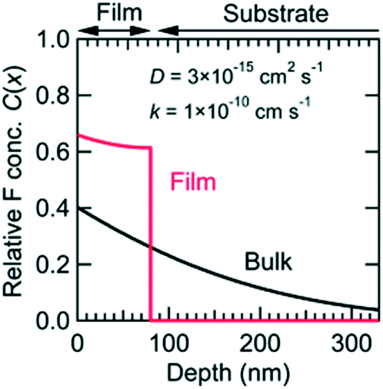 | ||
| Fig. 5 Relative fluorine concentration (C(x)) vs. depth (x) curves after topotactic reaction, calculated for 80 nm thick thin film and bulk sample. The details are described elsewhere.68 Reproduced with permission from ref. 69. Copyright 2014, The Royal Society of Chemistry. | ||
Topotactic reactions are sometimes reversible. Zhang et al. reported that ordered oxygen vacancies in semiconducting rhombohedral SrCoO2.8 are easily compensated for by annealing in air to form metallic cubic perovskite SrCoO3, and restored by further annealing in vacuum.70 Yoshimatsu et al. succeeded in reversible control of the topotactic reaction of Li+ ions in LiTi2O4 epitaxial thin film as the anode in a Li-ion battery structure using an electrochemical method.71 The superconductivity of LiTi2O4 was suppressed by intercalating Li+ ions, whereas it was recovered by successively deintercalating Li+ ions.
3 Engineering of functionality
Lattice structures of epitaxial thin films are modulated by underlying substrates and/or epitaxially stacked adjacent layers (Fig. 1). Because the lattice structure significantly influences various physical properties of oxides, such structural modulations are useful to conduct engineering of functionality. For example, ferroelectricity in ionic crystals is sensitive to lattice modulation because lattice strain directly affects the polarization usually originating from atomic displacement.72,73 Structural engineering is also effective to control magnetism because of the crystal field splitting governed by lattice symmetry and the exchange coupling strongly depending on the bond length and tilt angle of M–O–M bonds (M: transition metal).74The bond length/angle and coordination state in a crystal unit can be varied via epitaxial growth, i.e. lattice distortion and polymorphism, respectively. It is possible to stabilize a coordination state of a metastable polymorph via lattice matching between film and substrate. Also, it is possible to maintain the mother compound structure even in the case of heavier impurity doping beyond its thermodynamic solubility limit, enabling very heavy doping in comparison with the bulk specimen. On the other hand, mismatch in lattice constants and/or symmetry between film and substrate causes strain in the film, resulting in lattice distortion under biaxial tensile/compressive strain, defect formation, and bond tilting. Such variations of bonding possibly cause a drastic change in the electronic structure and physical properties, especially when several electronic phases compete with each other. In this section, we will provide an overview of various examples of crystal engineering in oxide epitaxial films reported recently.
3.1 Metastable polymorphs
Increasing phase stability using lattice matching, called epitaxial force, is the basic idea in all studies of epitaxial growth. A polymorph is stabilized on specific substrates possessing a similar structure. This approach has been widely applied to find novel metastable phases and to investigate structure dependent physical properties.75TiO2 exhibits many functionalities by impurity doping and is one of the most extensively studied oxides that have many polymorphs: rutile, anatase, brookite, columbite, cotunnite, baddeleyite, and fluorite.76 The rutile and anatase phases are the primary and secondary most stable phases under atmospheric conditions, respectively. The two stable polymorphs can be selectively formed on different substrates: the rutile phase on α-Al2O3 substrate and the anatase on lattice-matched perovskite substrates such as LAO and STO.76,77 Thus, their physical properties can be compared easily. For example, the anatase structure is more favourable to acquire both high transparency (over 95% at a wavelength of 600 nm) and low resistivity (∼2 × 10⁻⁴ Ω cm at room temperature) by Nb doping (Fig. 6).78,79
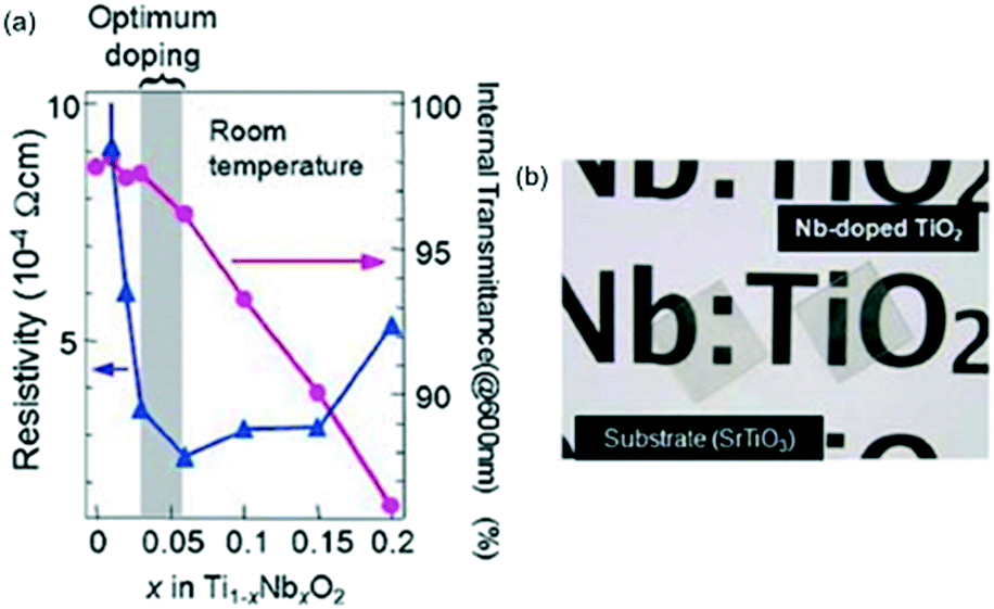 | ||
| Fig. 6 (a) Resistivity and internal transmittance (at a wavelength of 600 nm) of Ti1−xNbxO2 epitaxial thin films. (b) A photograph of STO substrate (left) and Ti0.94Nb0.06O2 epitaxial thin film on STO substrate (right). Reproduced with permission from ref. 79. Copyright 2010, WILEY-VCH. | ||
Another example is the recently achieved growth of high quality α-Ga2O3 (corundum structure) epitaxial thin films by mist-CVD.80 The α-phase is more attractive than the most stable β-phase from the viewpoint of functionality engineering, because of its capability to form a solid solution with other corundum oxides. For instance, wide range bandgap engineering from 3 to 9 eV is possible in solid solution with Al2O3 and In2O3, respectively.64 (AlxGa1−x)2O3 exhibited a linear variation of the bandgap between 5.3 and 8.8 eV, while (InxGa1−x)2O3 showed a variation of the bandgap between 3.8 and 5.3 eV with bowing due to the relatively small miscibility between In2O3 and Ga2O3. Control of magnetism is also possible in α-Ga2O3 by mixing with magnetic corundum oxides such as Cr2O3 and Fe2O3, and (Ga0.42Fe0.58)2O3 showed ferromagnetic properties at room temperature.81
The plane direction of the substrate can also be used to control the polymorphs. Lee et al. reported the selective growth of VO2 polymorphs on perovskite oxide substrates (Fig. 7).82 Due to uniaxial or biaxial lattice matching between the film and the substrates in addition to their lattice symmetry, tetragonal VO2 A-phase can be deposited on the (011) planes of STO and LAO, but monoclinic B- and M1- phases on the (001) and (111) planes, respectively. The R-phase appears through phase transition from the M1-phase at high temperature. Because VO2 shows largely varied physical properties such as electrical conductivity depending on the crystal structure (Fig. 7e), the selective growth of polymorphs is useful for their understanding and applications.
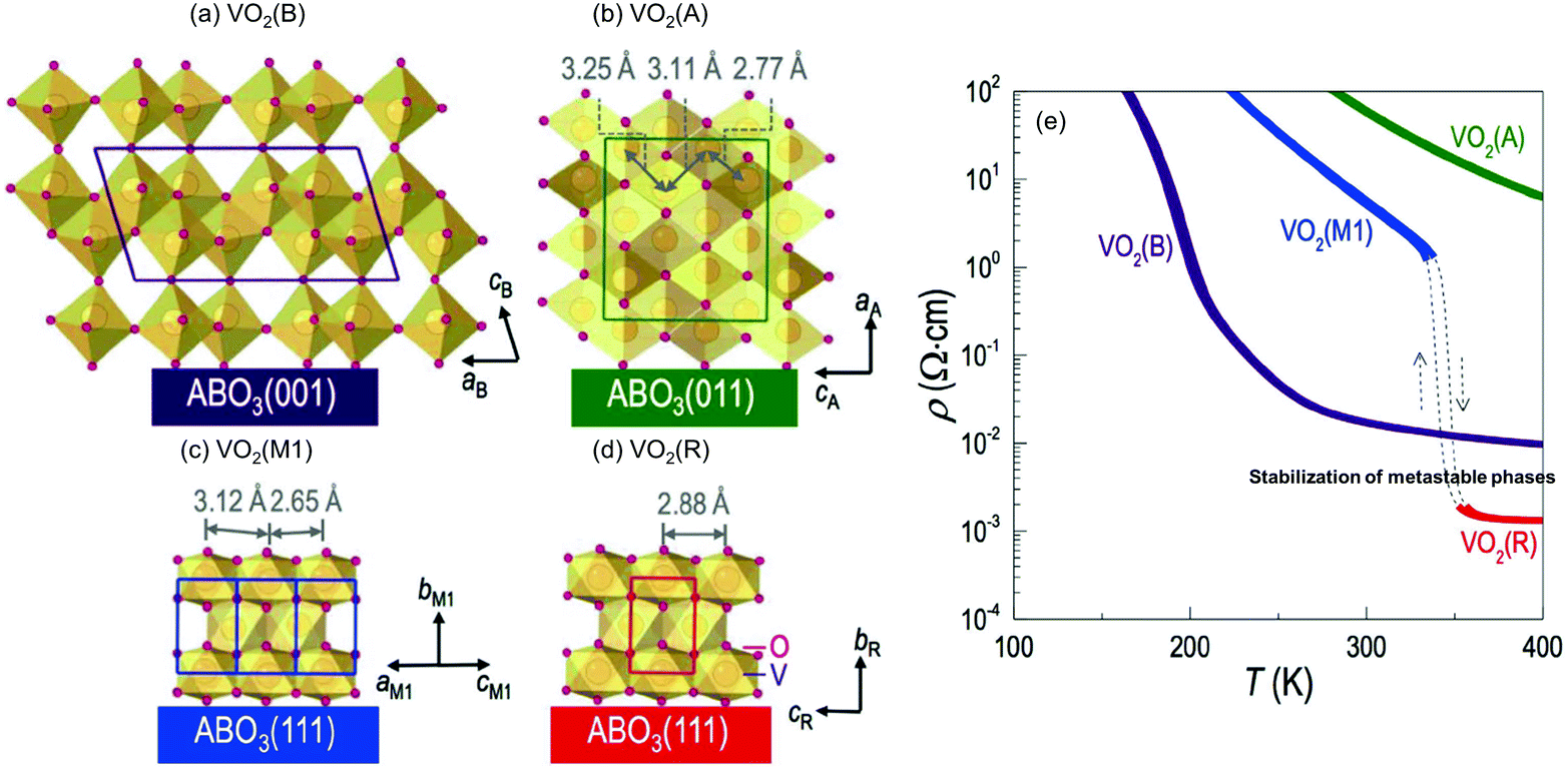 | ||
| Fig. 7 Schematic crystal structures of (a) VO2(B) on ABO3(001), (b) VO2(A) on ABO3(011), (c) VO2(M1), and (d) VO2(R) on ABO3(111) substrates. (e) Temperature dependence of resistivity for VO2(B), VO2(A), VO2(M1), and VO2(R) films. Reproduced with permission from ref. 82. Copyright 2016, Macmillan Publishers Limited. | ||
Epitaxial force can stabilize the metastable chemical composition, which otherwise results in phase separation. Lee et al. found a novel phase Sr2Ti7O14 in a Ti-rich STO epitaxial thin film.83 This metastable phase was obtained only in the case of a eutectic composition of 21 mol% SrO and 79 mol% TiO2 on the (111) planes of perovskite oxides such as STO and (LaAlO3)0.3–(SrAl0.5Ta0.5O3)0.7 (LSAT) at low growth temperature. Sr2Ti7O14 is composed of local STO-like layers separated by TiOx monolayers that have edge- and face-shared TiO6 octahedra with mixed valence Ti3+ and Ti4+. The superexchange interaction between the Ti3+ sites resulted in an antiferromagnetic insulating characteristic. It is noted that the thermal conductivity was as low as 1.3 W mK similar to glasses, in which the low thermal conductivity was attributed to the significant interlayer phonon scattering and the low out-of-plane electrical conductivity.
3.2 Doping beyond solubility limit
Impurity doping is a fundamental way to tailor functionalities in semiconductors including oxides. The ionic charge and size of dopants significantly affect the physical properties of the mother compound. The amount of impurity doping has an upper limitation, i.e. solubility limit, over which phase separation or structural transition occurs, prohibiting heavier doping possibly connected with the emergence of novel physical properties. The epitaxial force extends the solubility limit while preserving the mother structure.ZnO is an extensively investigated oxide semiconductor because of its promising potential for applications such as light emitting diodes (LEDs), photodetectors, and transparent transistors. To these ends, chemical doping is important to achieve p-type ZnO and bandgap engineering.84,85 For p-type doping, a wide range of dopants such as lithium, alkaline metals, copper, nitrogen, and phosphorus have been examined.84 For bandgap engineering, the dopants were usually divalent ions such as Mg2+ and Cd2+, resulting in bandgap widening and narrowing, respectively. Here, the most stable phase of MgO and CdO is the rock salt structure, constraining their thermodynamic solubility limit in wurtzite ZnO to as low as <4% and <2%, respectively.86 However, the solubility limits of MgO and CdO in ZnO were extended up to ∼50% and ∼70%, respectively, by epitaxial stabilization of the wurtzite structure on α-Al2O3 (0001), ScAlMgO4 (0001), and ZnO (0001), where the solubility limits depended on the growth method, conditions, and also the buffer layer.87–91 The extended solubility resulted in a broad range of bandgap engineering ranging from 1.8 to 4.5 eV for wurtzite (Zn,Mg,Cd)O. Also, bandgap widening by alloying with wurtzite BeO whose bandgap is 10.6 eV has been suggested,92 and a Be0.08Mg0.52Zn0.40O epitaxial thin film showed a bandgap of 5.11 eV.93 The largely variable bandgap of doped ZnO is now applicable for barrier layers of quantum wells in LEDs, the semiconducting layer of Schottky photodetectors, the acceptor layer of solar cells, and so on.85,94,95
Epitaxial stabilization of a doped semiconductor beyond the solubility limit of impurities sometimes leads to a new class of compounds, e.g. oxide-based diluted magnetic semiconductors such as transition metal doped ZnO, and a high temperature diluted ferromagnetic semitransparent semiconductor (Ti,Co)O2 with anatase and rutile types, discovered using the combinatorial approach.96–98 (Ti,Co)O2 shows a large magneto-optical effect in the ultraviolet-visible region and an anomalous Hall effect, and its magnetism can be controlled between paramagnetic and ferromagnetic states at room temperature by an electric field effect as well as chemical carrier doping (Fig. 8a and b),99,100 representing an electron carrier-mediated exchange interaction. Although divalent Co has been supposed to substitute the Ti site, a recent study of X-ray fluorescence holography indicated a local suboxidic coordination of CoO2Ti4 (Fig. 8d and f) in ferromagnetic rutile (Ti,Co)O2, whereas ordinary substitution of Co at the rutile Ti site was observed in paramagnetic (Ti,Co)O2 with low Co concentration (Fig. 8c and e).101 In spite of the unclear relationship between the high temperature ferromagnetism and the suboxide structure, this result suggests that formation of hidden local structures in doped oxides is a new strategy to design novel functionalities.
 | ||
| Fig. 8 (a) Magnetic-field dependence of the anomalous Hall conductivity σAH for anatase Ti0.90Co0.10O2−δ films at 300 K, measured at different gate voltages (VGs) using an electric double layer transistor. The values of electron density n at each VG are also shown. Reproduced with permission from ref. 100. Copyright © 2011 by the American Association for the Advancement of Science. (b) Anomalous Hall conductivity σAH at 300 K for anatase Ti0.90Co0.10O2−δ films grown in various oxygen pressures. Reproduced with permission from ref. 99. Copyright © 2011 American Institute of Physics. (c and d) Real-space images around Co in (c) rutile Ti0.09Co0.01O2 and (d) Ti0.95Co0.05O2 films reconstructed from X-ray fluorescence holograms. (e and f) Structure models obtained from the images in (c) and (d), respectively. Reproduced with permission from ref. 101. Copyright 2016, AIP Publishing. | ||
3.3 Unusual valence state
Owing to the advanced thin film techniques introduced in section 2, unusual valence states can be stabilized in thin films. Since an unusual valence state could lead to unconventional electronic states, chemical control of such valences is a possible way to find novel functionalities.Recently, epitaxial thin films of rock salt YO with unstable Y2+ (4d1) were synthesized using the non-equilibrium condition of the PLD process.102 Here, Y metal was used as a target and the unusual valence state was attained under precise control of minute partial oxygen pressure during growth by using Ar/O2 mixed gas. In contrast with the band insulator Y2O3 with Y3+, YO behaved as a narrow gap semiconductor and exhibited tuneable electrical conduction as a function of the amount of oxygen vacancy. The magnetoresistance showed weak antilocalization behaviour, which is attributed to strong spin–orbit coupling in the conducting 4d electrons.
ThCr2Si2 type R2O2Bi (R = rare earth or Y) has another unusual valence compound with a Bi2− square net, recently synthesized in a polycrystalline-powder form.103 To obtain epitaxial thin films of Y2O2Bi, reductive solid phase epitaxy was adopted.104 Y and Bi powders sandwiched between PLD-deposited Y2O3 amorphous films on CaF2 substrates were subjected to two-step heating in an Ar + H2 flow: the first low-temperature heating for alloying Bi and Y to reduce Bi by Y with a low redox potential, and the second high-temperature heating for solid phase epitaxy of the Y2O2Bi phase. This method was significantly improved by one step in situ heating of multilayer precursor [Y/Bi/Y2O3]25 with sub-nanometre layers (Fig. 9).105 The obtained films possessed high crystallinity and a flat surface, which allowed observation of intrinsic magnetoresistance reflecting the 2D nature and strong spin–orbit interaction of the Bi2− square net. Furthermore, this investigation resulted in the discovery of 2 K superconductivity in bulk Y2O2Bi polycrystal with excess oxygen.106
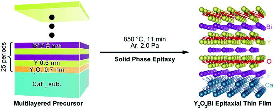 | ||
| Fig. 9 Schematic illustration of the synthetic procedure of Y2O2Bi epitaxial thin film via solid phase epitaxy. Reproduced with permission from ref. 105. Copyright 2015, American Chemical Society. | ||
3.4 Anion substitution
Instead of cation substitution in complex oxides frequently used for chemical modification, anion substitution is prevailing as an alternative route to synthesize new functional compounds. Hydride (H−), fluoride (F−), and nitride (N3−) ions can substitute oxygen sites in oxides owing to their similar ionic radii, thus mixed-anion oxides such as oxyhydrides, oxyfluorides, and oxynitrides have been synthesized with a broad range of chemical compositions and crystal structures.107 However, the fundamental properties of these mixed-anion oxides have been scarcely investigated because of the difficulty in high quality synthesis. Topotactic synthesis usually used for bulk specimens requires severe synthetic conditions such as high temperature and pressure for the reaction between stable oxide precursors and anion sources, resulting in an uncontrollable composition, structure, and homogeneity. In contrast, epitaxial thin film growth has several advantages such as a homogeneous milder post-deposition reaction,69 direct synthetic route under finely tuned conditions,108 and structural stabilization via epitaxial force.109,110Oxyhydride epitaxial films were prepared by reaction of oxide precursor films with hydration reagents such as CaH2. The hydride ion serves as an electron donor enabling heavy and tuneable electron doping. Yajima et al. and Bouilly et al. reported insulator-to-metal transition in ATiO3−xHx (A = Ca, Sr and Ba) epitaxial thin films by hydridation,111,112 in which the electrical conductivity was systematically tuned in the range of 0 ≤ x ≤ 0.5. The same group transformed an antiferromagnetic insulator EuTiO3 epitaxial thin film into a ferromagnetic metal EuTiO2.79H0.21 film with a Curie temperature of 12 K,113 which is higher than those of EuTiO3−δ, (Eu,La)TiO3, and Eu(Ti,Cr)O3, suggesting a smaller chemical disorder in EuTiO2.79H0.21. Katayama et al. obtained the first non-layered perovskite Sr–Co–O system, c-axis oriented SrCoOxHy (x = 1.6 ± 0.3, y = 1.2 ± 0.2) film, from brownmillerite SrCoO2.5 film by topotactic reaction with CaH2.114 Here, SrCoOxHy was formed not on LSAT substrate but on STO substrate with a smaller lattice mismatch owing to the epitaxial stabilization. The shorter b- and c-axis length (0.370 and 0.3702 nm) than the a-axis length (0.416 nm) indicated the preferential formation of a 2D Co–H–Co network in the bc plane rather than random 3D distribution of hydrogen, probably causing the splitting of t2g orbitals and bandgap widening from 0.35 eV of SrCoO2.5 to 2.1 eV of SrCoOxHy.
Moon et al. reported the fluorination of brownmillerite SrFeO3−δ (δ ∼ 0.5) into perovskite oxyfluoride SrFeO3−αFγ.115 Poly(vinylidene fluoride) (PVDF) spin-cast on the film was used as a fluorination reagent by annealing in an oxygen flow at 600 °C. SrFeO3−αFγ was semiconducting with a mixed valence state of Fe3+ and Fe4+, reflecting the insulating SrFeO3−δ with Fe3+ and metallic SrFeO3 with Fe4+, respectively. Katayama et al. reported SrFeO3−xFx epitaxial thin films by reaction of SrFeO3−δ thin film with spatially isolated PVDF in an Ar gas flow at a low temperature of 100–270 °C.69 The fluorine content in the SrFeO3−xFx films increased with increasing reaction temperature up to 270 °C, and decomposed into SrF2 and Fe3O4 at higher temperature. The fluorination reaction was promoted more by a larger amount of oxygen vacancy in SrFeO3−δ, and the fluorine amount x was widely varied in the range of 0.8 ≤ x ≤ 1.5.
Highly stable oxynitrides in comparison with oxyhydrides and oxyfluorides have been widely investigated as pigments, photocatalysts, and phosphors due to their bandgap harvesting visible and ultraviolet light.116 Since nitrogen ions are difficult to introduce into oxides with topotactic reactions partly due to the very low diffusion coefficient, the oxynitrides are usually powder specimens. Thus, the electrical properties have been scarcely investigated. In the case of epitaxial thin films, nitrogen can be in situ incorporated into oxides during film deposition by reactive rf magnetron sputtering,117 pulsed reactive crossed beam laser ablation,118 and other epitaxy techniques. Such thin films enable various characterization techniques.
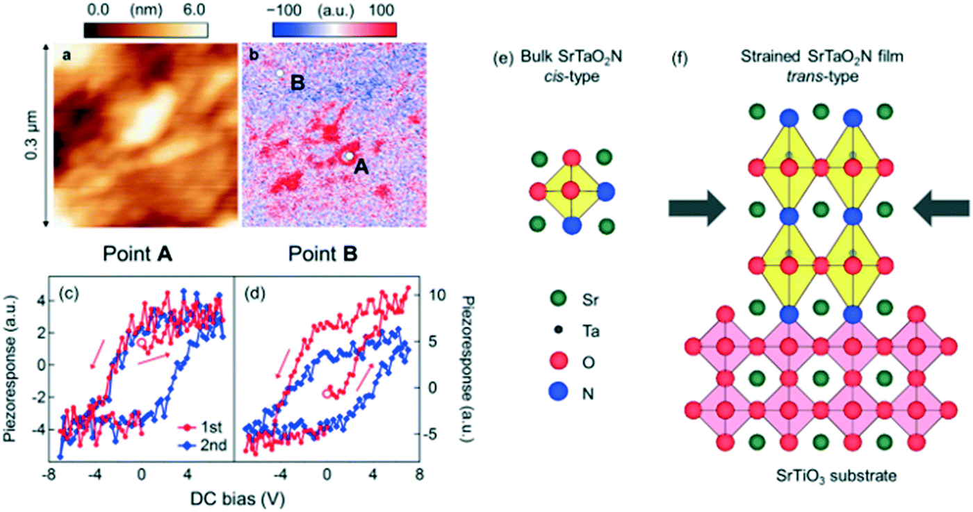
The nitrogen plasma assisted pulsed laser deposition (NPA-PLD) method was adopted for perovskite CaTaO2N epitaxial thin film.107 In this method, nitrogen radicals were supplied from a plasma source during deposition of CaTaO2N film on an STO substrate, where a Ca2Ta2O7 sintered target was used. Compared to film specimens obtained by other methods,119,120 the CaTaO2N film showed smaller dielectric loss probably due to the high crystallinity and chemical homogeneity. A SrTaO2N epitaxial thin film synthesized with the same method showed small classical ferroelectric regions surrounded by a relaxor-like matrix (Fig. 10a–d).109 This result is in stark contrast to paraelectric or wholly relaxor-like bulk SrTaO2N specimens,119,121 possibly caused by stabilization of a trans-type anion coordination in the compressively strained epitaxial thin film according to the first principles calculation (Fig. 10e and f). Such strain engineering on anion coordination can be a new approach to tailor novel functionalities in mixed-anion oxide epitaxial thin films. Electrically conductive oxynitrides are also available with NPA-PLD. Suzuki et al. synthesized metastable anatase TaON epitaxial thin film with the aid of epitaxial stabilization.122 TaON showed a rather high mobility of ∼17 cm2 V−1 s−1 at room temperature with an electron density of 3.7 × 1019 cm−3 supplied from oxygen vacancy. Electrical properties such as electrical conductivity and magnetism were controlled by the nitrogen content in films like hydride in oxyhydrides. Takahashi et al. synthesized AX-type CoOxNy epitaxial thin film, in which the anion ratio y/(x + y) was systematically controlled in the range from 0 to 0.63.123 CoOxNy showed a structural phase transition from rock salt (y/(x + y) < 0.5) to zinc blend (y/(x + y) > 0.5) structure. For the former, insulator-to-metal transition was induced by increasing nitrogen up to y/(x + y) > 0.34, concomitant with a drastic increase in saturation magnetization near the phase boundary. Recently, a topotactic synthetic route for oxynitrides was developed by Yajima et al.124 BaTiO3−xHx precursor was transformed to BaTiO3−xN2x/3via nitridation with NH3 at an unusually low temperature of 375–550 °C, by utilizing the lability of hydride ions in oxyhydrides. The BaTiO0.2N0.4 epitaxial thin film maintained the ferroelectric nature of BaTiO3.
 | ||
| Fig. 10 (a) Topographic and (b) piezoresponse images of SrTaO2N epitaxial thin film. (c and d) Local piezoresponse examined by switching spectroscopy at positions A and B in (b). (e and f) Schematics of (e) unstrained bulk SrTaO2N with a cis-type anion arrangement and (f) tetragonally strained SrTaO2N thin film with a trans-type anion arrangement epitaxially stabilized on SrTiO3 substrate. Reproduced with permission from ref. 109. Copyright 2014, Macmillan Publishers Limited. | ||
3.5 Epitaxial strain
Since the demonstration of enhanced Curie temperature in compressively strained BaTiO3 epitaxial thin films,125 the effects of epitaxial strain caused by lattice mismatch between film and substrate have been extensively investigated for various (quantum) ferroelectric compounds such as STO,126 Pb(Zr,Ti)O3,127 and BiFeO3,128 recently reviewed by Damodaran et al.129 Also, multiferroicity has been artificially generated by inducing ferroelectricity in magnetic compounds. Takahashi et al. reported single phase multiferroicity in ferromagnetic double perovskite La2NiMnO6 epitaxial thin film by appending ferroelectricity via lattice stretching along [111]cubic on STO substrate.130 It is noted that this ferroelectricity is driven by displacement of the A-site without lone pair electrons, as scarcely seen in perovskite oxides. Yun et al. reported high quality epitaxial thin films of metastable layered multiferroic Bi6FeCoTi3O18 on a conducting LaNiO3 buffer layer.131 LaNiO3 significantly stabilized the film crystallization by preventing the divergence of electrical potential due to spontaneous polarization of the film through charge screening. The film showed phase switching in piezoresponse at room temperature, probably induced by the compressive strain from the substrate.In addition to ferroelectricity, magnetism can also be controlled by strain because the bond angle between transition metal ions varies their exchange coupling, as demonstrated in (La,Sr)MnO3 thin film on perovskite substrates decades ago.132 Yang et al. reported an anomalous phase diagram of La1−xSrxCoO3 under epitaxial strain.133 Under tensile strain, ferromagnetism was induced in LaCoO3 thin film due to a superexchange interaction between high spin–low spin–high spin Co3+ ions. On the other hand, ferromagnetism was strongly suppressed in La1−xSrxCoO3 (x ∼ 0.2) thin film due to reduced double exchange coupling between Co3+ and Co4+ ions: the hole doping effect and local lattice strain caused by the introduction of Sr in addition to tensile strain assisted transition from high spin state Co3+ into low spin state Co4+ ions. Li et al. controlled interfacial magnetism between G-type antiferromagnetic SrMnO3 (001) and ferromagnetic (La,Sr)MnO3 (001) epitaxial thin films via octahedral tilting tuned by strain as a function of SrMnO3 thickness and type of substrate.134 Here, the Dzyaloshinskii–Moriya (DM) interaction of the bilayer is expressed as 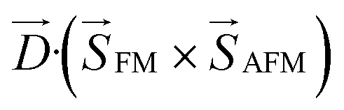 , where
  denotes the DM vector and
  and
and  are spin vectors of FM and AFM layers, respectively. The DM interaction is finite only in case of out-of-phase tilting along the [100] direction in the antiferromagnetic layer under a magnetic field along the [010] direction (Fig. 11a). As expected by first principles calculation that the out-of-phase tilting along the [100] direction is stabilized under tensile strain, the most tensilely (compressively) strained film with the smallest SrMnO3 thickness deposited on STO (LAO) showed the highest (lowest) exchange biases, and the strain effect relaxed gradually with increasing SrMnO3 thickness (Fig. 11b and c).
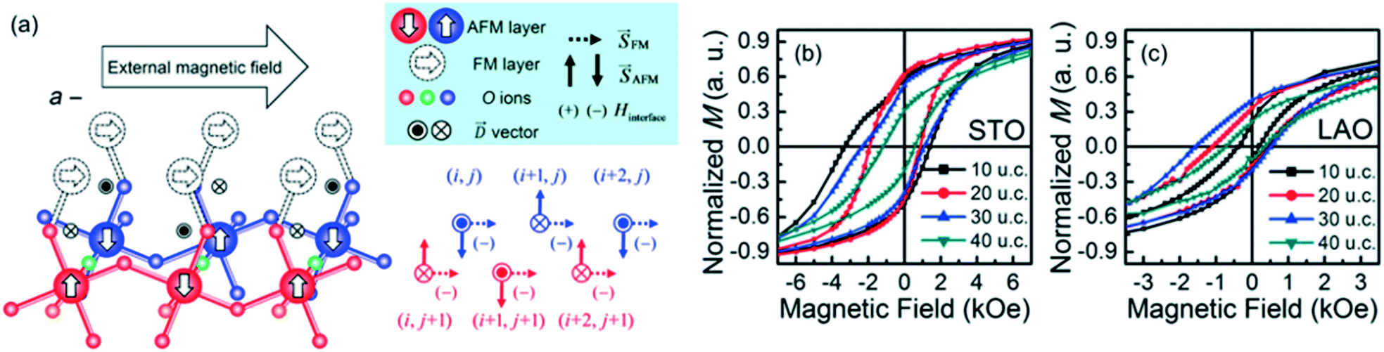 | ||
| Fig. 11 (a) Sketch of the G-type antiferromagnetic/ferromagnetic interface given for antiphase tilting about the [100] (a axis) with the sign of the Dzyaloshinskii–Moriya interaction term shown in the right simplified diagram for the whole interface. (b and c) Magnetization curves of (La,Sr)MnO3 (20 u.c.)/SrMnO3 (t) on STO (b) and LAO (c) for different SrMnO3 thicknesses (t = 10, 20, 30, and 40 u.c.). Reproduced with permission from ref. 134. Copyright 2015, Macmillan Publishers Limited. | ||
Intriguingly, an epitaxial strain effect on the physical properties was manifested not only at the film–substrate interface but also at the surface. Marín et al. reported significantly suppressed saturation magnetization and an enhanced coercive field in compressively or tensilely strained ferromagnetic (La,Ca)MnO3 epitaxial films.135 Electron holography revealed the presence of an about 20 nm thick antiferromagnetic layer around the surface region. As a consequence of the coupling effect between eg orbital ordering and Jahn–Teller distortions induced by strain, in addition to the relaxation of long-range interaction at the surface, the antiferromagnetic ordering emerged only at the surface, yielding the exchange bias.
Hirai et al. suggested that oxygen deficient materials are suitable for strain engineering of physical properties.136 Oxygen deficient perovskite SrFeO2.8 films with tensile strain showed metal-to-insulator transition accompanied by charge disproportionation of Fe3.66+ into Fe3+ and Fe4+ at 620 K far above that of the bulk specimen, 70 K. The amount of oxygen deficiency itself was varied by epitaxial strain. Petrie et al. reported the formation of intermediate oxidation states SrCoO3−δ between perovskite SrCoO3 and brownmillerite SrCoO2.5 under tensile strain.137 With increasing tensile strain from 1.0% to 4.2%, δ linearly increased from 0.1 to 0.25, resulting in ferromagnetic metal to antiferromagnetic insulator transition. According to calculation, tensile strain destabilized the ground state due to the reduced intercalation formation enthalpy of oxygen, giving a route to modify oxygen conduction in oxides. Farokhipoor et al. reported epitaxial strain control of cation deficient domain wall density in a multiferroic system.138 Tensilely strained TbMnO3 film on STO substrate with a lattice mismatch of 5% showed dense formation of the domain walls which occupy as high as 25% of total film volume to release the large strain (Fig. 12a). At the domain wall, Tb was replaced by Mn (Fig. 12b and c) to enhance net magnetization (Fig. 12d and e). Such artificial control of local lattice structure can be used to form novel crystal structures and functionalities.
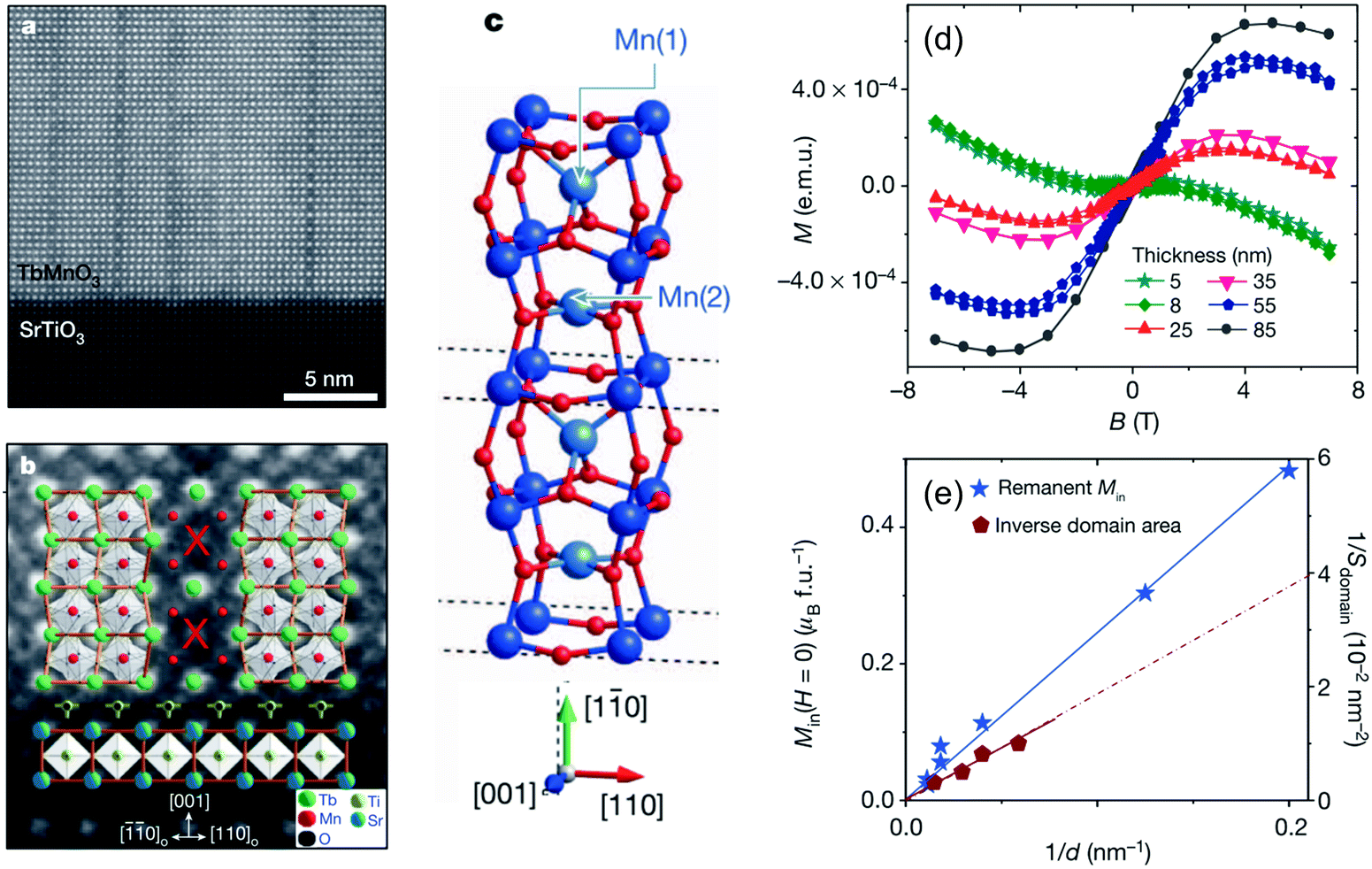 | ||
| Fig. 12 (a) HAADF-STEM image of TbMnO3–SrTiO3 interface. (b) Domain wall in TbMnO3 close to the interface with SrTIO3, superposed on the proposed atomic model. (c) Proposed columnar structure of substitutional Mn cations (light blue) at domain wall. (d) In-plane magnetization curves at 10 K for TbMnO3 films with various thicknesses. (e) Remanent magnetization versus the inverse of film thickness. The inverse domain area (or density of domain walls) is also plotted. Reproduced with permission from ref. 138. Copyright 2014, Macmillan Publishers Limited. | ||
3.6 Defect formation
As mentioned in section 2, it is often difficult to transfer stoichiometric composition from source to film. Even in the case of PLD, off-stoichiometric thin films are often deposited. As reported by Ohnishi et al., laser fluence is one of the most significant factors that govern the film composition,139 suggesting that the kinetic energy of the chemical species during deposition influences the chemical composition in thin films by defect formation. Such defects in epitaxial films and heteroepitaxial structures usually cause undesired effects on the physical properties, but recently have been exploited to develop novel functionalities. Lee et al. controlled the amount and site of vacancies in STO thin films systematically by growth condition.140 The c-axis lattice constant, proportional to the amount of Sr vacancy, was increased by laser energy, while an insulator-to-metal transition accompanied by reduced transmittance was induced by introducing an oxygen vacancy via oxygen flow rate without significant change in the lattice parameter. Sarantopoulos et al. precisely controlled the amount of Sr and O vacancies in STO epitaxial thin films by changing the partial oxygen pressure during PLD growth.141 Uniform tetragonal distortion along 50 nm thick film due to Sr vacancy, in spite of the presence of film/substrate interfacial defects, resulted in splitting of t2g states coupled with the spin–orbit interaction. The lowered degeneracy was manifested as the emergence of an anomalous Hall effect and anisotropic magnetoresistance, similar to LAO/STO interfaces and quantum wells, possibly caused by long range magnetic ordering.Defect induced strain is an efficient way to modulate ferroelectricity like lattice mismatch induced strain. Damodaran et al. reported significant c-axis expansion of up to 4.1% in PLD-deposited stoichiometric BaTiO3 films with increasing laser fluence (Fig. 13a).142 This expansion was attributed to dipole formation from charged point defects along the out-of-plane direction in addition to the compressive epitaxial strain from GdScO3 substrates. These defects enhanced the Curie temperature up to 800 °C without impairing insulating properties (Fig. 13b and c).
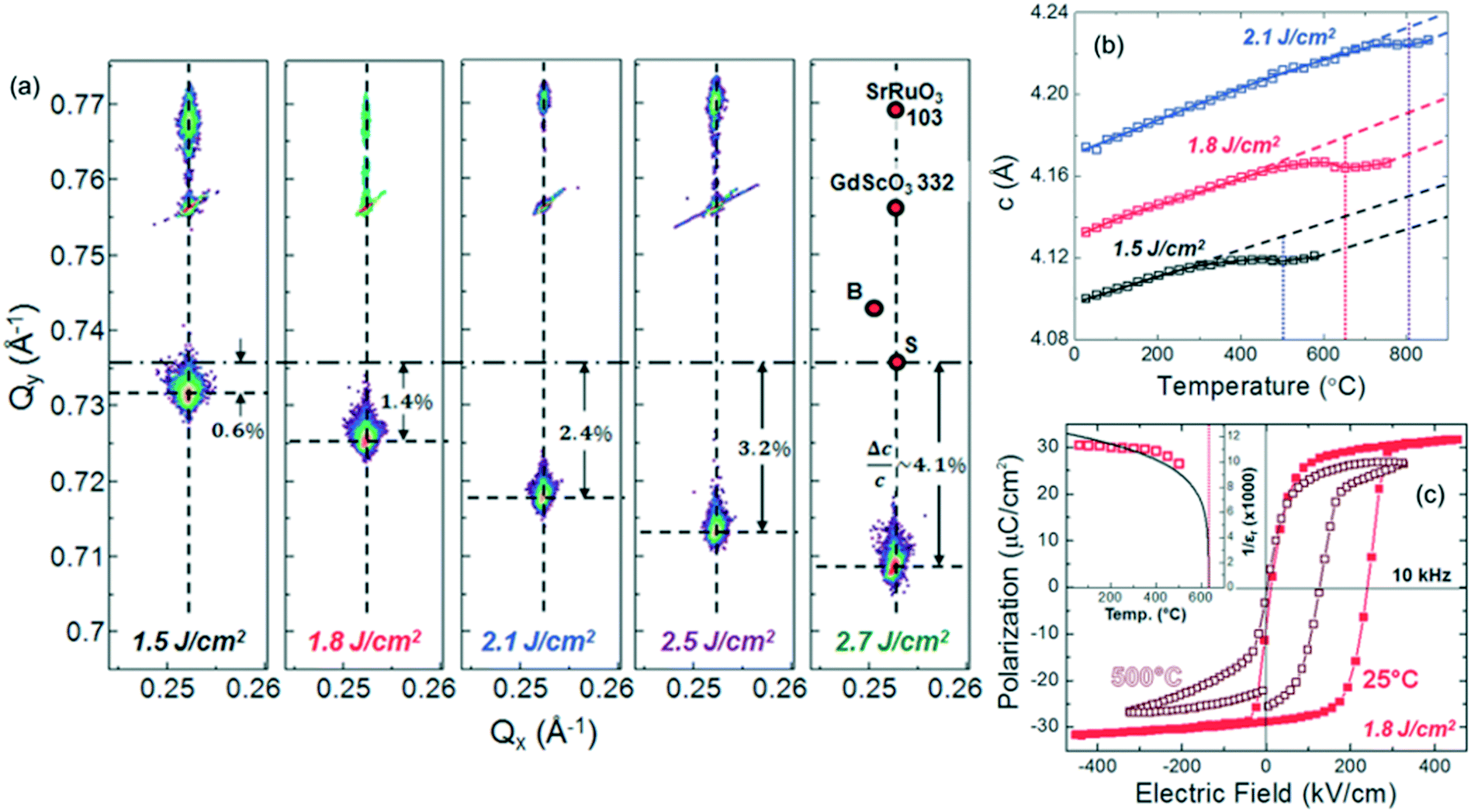 | ||
| Fig. 13 (a) Reciprocal space maps around the 103- and 332-diffractions of BaTiO3 films and GdScO3 substrate as a function of laser fluence of 1.5, 1.8, 2.1, 2.5, and 2.7 J cm−2. (b) Temperature dependence of out-of-plane c-axis lattice parameters with different laser fluences for BaTiO3/SrRuO3/GdScO3 (110) heterostructures. (c) Ferroelectric hysteresis loops for the heterostructure grown at 1.8 J cm−2, revealing the presence of strong polarization even at 500 °C. The inset shows the evolution of the polarization from 25 to 500 °C. Reproduced with permission from ref. 142. Copyright 2014, John Wiley & Sons, Inc. | ||
Recently, ferroelectric-like behaviours were observed using piezoelectric force microscopy in heterostructures composed of non-ferroelectric oxides such as STO, TiO2,143 and LAO.144 Sharma et al. investigated LAO epitaxial thin films deposited on the lattice-matched conducting Sr0.2Ca0.8RuO3 bottom layer on LSAT substrate.145 By excluding extrinsic effects such as surface charge effects and current induced electromechanical responses, the ferroelectric-like behaviour was attributed to bistable distributions of ions and oxygen-vacancies in the films. The stable distributions were switched not only by an external electric field but also by mechanical force with an atomic force microscope tip. The latter corresponds to a flexoelectric effect generating an internal electric field proportional to the applied stress. Such a ferroelectric-like response caused by ion/vacancy migration was suggested for potential switching applications with mechanical-write and electrical-read.
3.7 Substructure propagation
Chemical bonding across the film/substrate heterointerface is associated with not only lattice matching but also substructure propagation as seen in the octahedral rotation in perovskite heterostructures. The latter is an interesting effect because the chemical bonding angle significantly affects physical properties such as optical band gap, magnetism, and polarity.The propagation effects of octahedral rotation in perovskite heterostructures were suggested earlier than direct or indirect observation.146–149 Recently, Aso et al. directly observed in-phase octahedral rotation around the [001]ortho direction near the interface of perovskite SrRuO3 film on GaScO3 substrate, in which both crystals have a Pbmn orthorhombic structure.150 The RuO6 octahedron in the thin film was forced to rotate in order to match the rotation angle of the ScO6 octahedron in the substrate, whereas the topmost apical oxygen in the ScO6 octahedron was dragged from its original site because of their largely different octahedral tilt angle θ (θ = 168° and 156° for SrRuO3 and GdScO3, respectively). The substructure propagation was relieved within only 4 unit cells while the in-plane lattice parameter of the film was perfectly locked. The rotation angle in the film was controlled by inserting a buffer layer. In the case of the BaTiO3 buffer layer, SrRuO3 transformed into the tetragonal phase due to the large ionic radius of Ba, resulting in strong suppression of octahedral rotation.151 On the other hand, the tilt angle was controllably reduced by inserting a Ca0.5Sr0.5TiO3 layer with different thicknesses from 1 u.c. to 4 u.c.: θ = 180° for 4 u.c. as in the case of the BaTiO3 buffer layer (Fig. 14a–h).152 Interestingly, the rotation angle was constant along the whole thickness of the SrRuO3 layer probably due to the bistability of the orthorhombic phase (θ = 168°) and tetragonal phase (θ = 180°). The influence of the octahedral rotation angle on the electronic structure was manifested as magnetic anisotropy of ferromagnetic SrRuO3 thin films. The easy magnetization axis was rotated by about 45° at θ ≈ 175° (Fig. 14i). The details were recently reviewed elsewhere.153
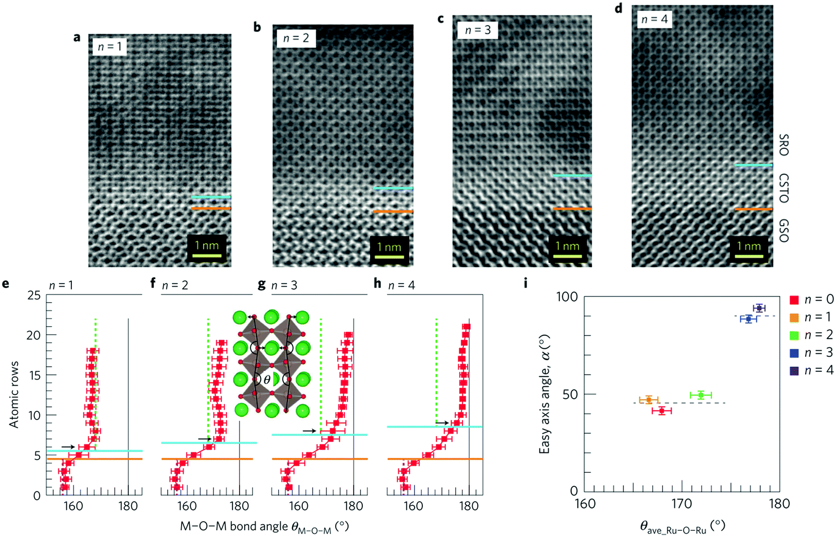 | ||
| Fig. 14 (a–d) ABF-STEM images for the (a) n = 1, (b) n = 2, (c) n = 3, and (d) n = 4 SrRuO3/[Ca0.5Sr0.5TiO3]n/GdScO3 heterostructures. Blue and orange lines denote SrRuO3/Ca0.5Sr0.5TiO3 and Ca0.5Sr0.5TiO3/GdScO3 interfaces, respectively. (e–h) M–O–M bond angle θM–O–M (M = Sc, Ti, and Ru) as a function of atomic position in (e) n = 1, (f) n = 2, (g) n = 3 and (h) n = 4. (i) Magnetization easy axis angle α as a function of the Ru–O–Ru bond angle θave_Ru–O–Ru in the SrRuO3 layer. Reproduced with permission from ref. 152. Copyright 2014, Macmillan Publishers Limited. | ||
The substructure propagation is observed in various epitaxial thin films. Liao et al. observed a large octahedral rotation propagated from NdGaO3 substrates to adjacent 4 u.c. layers in (La,Sr)MnO3 epitaxial thin films.154 The magnetic easy axis was rotated from the original b-axis in bulk to the a-axis as was not observed in the films on the STO buffer layer, indicating that the large octahedral rotation induces the magnetic anisotropy rotation. Qiao et al. investigated the influence of symmetry mismatch on LaCoO3 epitaxial thin films.155 Magnetism significantly depended on the LaCoO3 film thickness on STO substrates: moderately correlated diamagnetic behaviour for 5 u.c. thick film and strongly correlated ferromagnetic behaviour for 15 u.c. thick film (Fig. 15a and d). The strong correlation for the latter can be rationalized by the decrease of crystal field splitting caused by expansion of CoO6 octahedra under tensile strain. The accompanying octahedral tilt decreases Co–O bond covalency which favours magnetic order (Fig. 15c and e). On the other hand the moderate correlation and diamagnetism in the thinner film was caused by suppressed octahedral tilting due to mismatch in the octahedral rotation angle (Fig. 15b and e). The authors proposed that heteroepitaxial strain introduces volume change in the octahedron more efficiently than chemical substitution does.
 | ||
| Fig. 15 (a) Temperature dependence of magnetization for LaCoO3/STO films and superlattice at 1000 Oe under field-cooling. The top inset shows magnetic hysteresis curves at 5 K. The bottom inset shows low-magnification cross sectional HAADF images. (b and c) HAADF (left)/ABF (right) images of (b) 5 u.c. and (c) 15 u.c. LaCoO3 films in the [110] projection. Red dots represent the oxygen columns in LaCoO3 film. (d) Magnetization and structural parameters for LaCOO3 films as well as referential data of bulk LaCoO3 and 20 nm epitaxial LaCoO3 on STO and LAO substrates. (e) Bond valence of Co as a function of cell volume for different perovskite Co3+ bulk compounds and epitaxial LaCoO3, with and without octahedral rotations, based on the experimental structures. The inset shows schematic changes in unit cell volume and CoO6 octahedral distortion for ACoO3 bulk perovskites and epitaxial LaCoO3 films. Reproduced with permission from ref. 155. Copyright 2015, American Chemical Society. | ||
Out-of-plane atomic displacement of substructure in a polar substrate also propagates into the film. Chen et al. investigated the structural change in ferromagnetic (La,Sr)MnO3 epitaxial films on 20 u.c. thick ferroelectric BaTiO3 bottom layers.156 In the case of the spontaneous polarization in BaTiO3 backward to the interface, hole accumulation and structural asymmetry at the interface caused a shift of Mn ions in phase with that of Ti ions in BaTiO3 accompanied by a small decrease of c/a, resulting in broken degeneracy of Mn eg orbitals to stabilize the dx2−y2 orbital (Fig. 16a, c and e). In the case of the opposite spontaneous polarization, hole depletion caused tetragonal distortion (c/a > 1) of the (La,Sr)MnO3 unit cell, resulting in broken degeneracy of Mn eg orbitals to destabilize the dx2−y2 on the contrary (Fig. 16b and d). Accordingly, the d electron population in the transition metal oxide film was controlled by switching spontaneous polarization in the adjacent ferroelectric layer. Later, Preziosi et al. observed the change in electron population of Mn eg orbitals by polarization switching in (La,Sr)MnO3 epitaxial thin film on Pb(Zr,Ti)O3 layer by means of X-ray linear dichroism (Fig. 16f and g).157
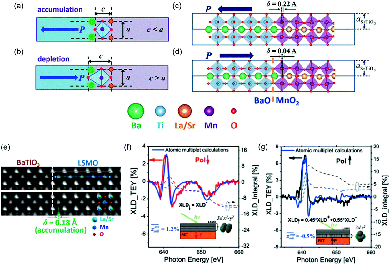 | ||
| Fig. 16 (a and b) Schematic BaO/MnO2 interfaces of BaTiO3/(La,Sr)MnO3 heterostructure in (a) accumulation and (b) depletion states. The purple and light blue parts represent (La,Sr)MnO3 and BaTiO3, respectively. (c and d) Relaxed atomic structure of the interfaces in (c) accumulation and (d) depletion states from first-principles calculations. (e) ABF image of the interface in accumulation state. Reproduced with permission from ref. 156. Copyright© 2014 American Chemical Society. (f and g) Experimental and theoretical X-ray linear dichroism spectra for a (La,Sr)MnO3 epitaxial film on Pb(Zr,Ti)O3 in (f) accumulation and (g) depletion states. Reproduced with permission from ref. 157. Copyright 2015, American Physical Society. | ||
4 Outlook
In this review, we presented recent advances in growth techniques of functional oxide epitaxial thin films and their crystal engineering for novel functionalities. Atomic-scale control of films is possible from aspects of both chemical composition and crystal structure. Accordingly, research fields utilizing oxide epitaxy technology are rapidly spreading: oxide ionics,158–161 interface phenomena16 such as formation of 2DEG162–166 and topological states,167 low dimensional electronics,168–170 quantum effects,171 and 4d/5d oxide electronics.172,173 In order to develop these fields further, comprehensive understanding of not only the film growth processes including metastable structure formation and ionic migration but also the atomic-scale electronic states at the interface and the ultrathin layer and of interplay between electron, spin, and orbital are indispensable. To this end, cutting edge thin film growth methods and atomic-scale analytical tools are important. Crystal engineering of functional oxides is important for not only basic science but also practical applications, contributing to the discovery of novel phenomena and invention of next generation applications. In addition, the development of oxide thin film epitaxy will merge modern silicon and III–V semiconductor technologies and oxide electronics. The crystal engineering of oxides even on non-oxide substrates is possible.174,175 Also, organic–inorganic hybrid devices are under investigation.176,177 The combination of oxides with different classes of materials would further expand these emerging research fields.Acknowledgements
This work was in part supported by Core Research for Evolutionary Science and Technology of Japan Science and Technology Agency and JSPS KAKENHI (26600091, 26105002).References
- J. Heber, Nature, 2009, 459, 28–30 CrossRef CAS PubMed
.
-
Functional Metal Oxides: New Science and Novel Applications, ed. S. B. Ogale, T. V. Venkatesan and M. Blamire, Wiley-VCH, 2013 Search PubMed
- M. Lorenz, M. S. Ramachandra Rao, T. Venkatesan, E. Fortunato, P. Barquinha, R. Branquinho, D. Salgueiro, R. Martins, E. Carlos, A. Liu, F. K. Shan, M. Grundmann, H. Boschker, J. Mukherjee, M. Priyadarshini, N. Das Gupta, D. J. Rogers, F. H. Teherani, E. V. Sandana, P. Bove, K. Rietwyk, A. Zaban, A. Veziridis, A. Weidenkaff, M. Muralidhar, M. Murakami, S. Abel, J. Fompeyrine, J. Zuniga-Perez, R. Ramesh, N. A. Spaldin, S. Ostanin, V. Borisov, I. Mertig, V. Lazenka, G. Srinivasan, W. Prellier, M. Uchida, M. Kawasaki, R. Pentcheva, P. Gegenwart, F. Miletto Granozio, J. Fontcuberta and N. Pryds, J. Phys. D: Appl. Phys., 2016, 49, 433001 CrossRef
- H. Hosono, Thin Solid Films, 2007, 515, 6000–6014 CrossRef CAS
- L. Martin, Y. Chu and R. Ramesh, Mater. Sci. Eng., R, 2010, 68, 89–133 CrossRef
- K. F. Wang, J.-M. Liu and Z. F. Ren, Adv. Phys., 2009, 58, 321–448 CrossRef CAS
- K. D. Kreuer, Annu. Rev. Mater. Res., 2003, 33, 333–359 CrossRef CAS
- M. Imada, A. Fujimori and Y. Tokura, Rev. Mod. Phys., 1998, 70, 1039–1263 CrossRef CAS
- A. P. Ramirez, Science, 2007, 315, 1377–1378 CrossRef PubMed
- J. G. Bednorz and K. A. Muller, Z. Phys. B: Condens. Matter, 1986, 64, 189–193 CrossRef CAS
- H. Koinuma, Solid State Ionics, 1998, 108, 1–7 CrossRef CAS
- Crystal Engineering of High-Tc-related Oxide Films (special issue), ed. H. Koinuma, MRS Bull., 1994, vol. 19 Search PubMed.
- H. Koinuma, Thin Solid Films, 2005, 486, 2–10 CrossRef CAS
- M. Kawasaki, Bull. Chem. Soc. Jpn., 2013, 86, 1341–1358 CrossRef CAS
- F. J. Wong and S. Ramanathan, J. Vac. Sci. Technol., A, 2014, 32, 40801 Search PubMed
- H. Y. Hwang, Y. Iwasa, M. Kawasaki, B. Keimer, N. Nagaosa and Y. Tokura, Nat. Mater., 2012, 11, 103–113 CrossRef CAS PubMed
- M. Ziese and I. Vrejoiu, Phys. Status Solidi RRL, 2013, 7, 243–257 CrossRef CAS
- H.-J. Liu, W.-I. Liang, Y.-H. Chu, H. Zheng and R. Ramesh, MRS Commun., 2014, 4, 31–44 CrossRef CAS
- J. L. Macmanus-Driscoll, Adv. Funct. Mater., 2010, 20, 2035–2045 CrossRef CAS
- J. J. Cuomo, D. L. Pappas, J. Bruley, J. P. Doyle and K. L. Saenger, J. Appl. Phys., 1991, 70, 1706–1711 CrossRef CAS
- M. N. R. Ashfold, F. Claeyssens, G. M. Fuge and S. J. Henley, Chem. Soc. Rev., 2004, 33, 23–31 RSC
- H. M. Christen and G. Eres, J. Phys.: Condens. Matter, 2008, 20, 264005 CrossRef CAS PubMed
- R. K. Singh and J. Narayan, Phys. Rev. B: Condens. Matter Mater. Phys., 1990, 41, 8843–8859 CrossRef
- T. Ohnishi, H. Koinuma and M. Lippmaa, Appl. Surf. Sci., 2006, 252, 2466–2471 CrossRef CAS
- S. Ohashi, M. Lippmaa, N. Nakagawa, H. Nagasawa, H. Koinuma and M. Kawasaki, Rev. Sci. Instrum., 1999, 70, 178–183 CrossRef CAS
- T. Koida, D. Komiyama, H. Koinuma, M. Ohtani, M. Lippmaa and M. Kawasaki, Appl. Phys. Lett., 2002, 80, 565–567 CrossRef CAS
- H. Koinuma and I. Takeuchi, Nat. Mater., 2004, 3, 429–438 CrossRef CAS PubMed
- M. Lippmaa, N. Nakagawa, M. Kawasaki, S. Ohashi and H. Koinuma, Appl. Phys. Lett., 2000, 76, 2439–2441 CrossRef CAS
- T. M. Shaw, A. Gupta, M. Y. Chern, P. E. Batson, R. B. Laibowitz and B. A. Scott, J. Mater. Res., 1994, 9, 2566–2573 CrossRef CAS
- T. Ohnishi, D. Komiyama, T. Koida, S. Ohashi, C. Stauter, H. Koinuma, A. Ohtomo, M. Lippmaa, N. Nakagawa, M. Kawasaki, T. Kikuchi and K. Omote, Appl. Phys. Lett., 2001, 79, 536–538 CrossRef CAS
-
Handbook of Thin Film Deposition (Third Edition), ed. K. Seshan, Elsevier, 2012 Search PubMed
- V. S. Smentkowski, Prog. Surf. Sci., 2000, 64, 1–58 CrossRef CAS
- P. Willmott, Prog. Surf. Sci., 2004, 76, 163–217 CrossRef CAS
- P. J. Martin, J. Mater. Sci., 1986, 21, 1–25 CrossRef CAS
- E. Bousquet, M. Dawber, N. Stucki, C. Lichtensteiger, P. Hermet, S. Gariglio, J.-M. Triscone and P. Ghosez, Nature, 2008, 452, 732–736 CrossRef CAS PubMed
- J. Garcia-Barriocanal, A. Rivera-Calzada, M. Varela, Z. Sefrioui, E. Iborra, C. Leon, S. J. Pennycook and J. Santamaria, Science, 2008, 321, 676–680 CrossRef CAS PubMed
- F. Baiutti, G. Christiani and G. Logvenov, Beilstein J. Nanotechnol., 2014, 5, 596–602 CrossRef PubMed
- A. A. Baker, W. Braun, G. Gassler, S. Rembold, A. Fischer and T. Hesjedal, Rev. Sci. Instrum., 2015, 86, 043901 CrossRef CAS PubMed
- K. Horiba, H. Ohguchi, H. Kumigashira, M. Oshima, K. Ono, N. Nakagawa, M. Lippmaa, M. Kawasaki and H. Koinuma, Rev. Sci. Instrum., 2003, 74, 3406–3412 CrossRef CAS
- C. D. Theis, J. Yeh, D. G. Schlom, M. E. Hawley and G. W. Brown, Thin Solid Films, 1998, 325, 107–114 CrossRef CAS
- B. Jalan, P. Moetakef and S. Stemmer, Appl. Phys. Lett., 2009, 95, 32906 CrossRef
- A. Tsukazaki, S. Akasaka, K. Nakahara, Y. Ohno, H. Ohno, D. Maryenko, A. Ohtomo and M. Kawasaki, Nat. Mater., 2010, 9, 889–893 CrossRef CAS PubMed
- B. Jalan, R. Engel-Herbert, N. J. Wright and S. Stemmer, J. Vac. Sci. Technol., A, 2009, 27, 461–464 CAS
- J. Son, P. Moetakef, B. Jalan, O. Bierwagen, N. J. Wright, R. Engel-Herbert and S. Stemmer, Nat. Mater., 2010, 9, 482–484 CrossRef CAS PubMed
- Y. Matsubara, K. S. Takahashi, M. S. Bahramy, Y. Kozuka, D. Maryenko, J. Falson, A. Tsukazaki, Y. Tokura and M. Kawasaki, Nat. Commun., 2016, 7, 11631 CrossRef CAS PubMed
- S. Vallejos, F. Di Maggio, T. Shujah and C. Blackman, Chemosensors, 2016, 4, 4 CrossRef
- T. Goto, J. Wuhan Univ. Technol., Mater. Sci. Ed., 2016, 31, 1–5 CrossRef CAS
- K. Haga, M. Kamidaira, Y. Kashiwaba, T. Sekiguchi and H. Watanabe, J. Cryst. Growth, 2000, 214–215, 77–80 CrossRef
- Y. Kuzminykh, A. Dabirian, M. Reinke and P. Hoffmann, Surf. Coat. Technol., 2013, 230, 13–21 CrossRef CAS
- K. Sawada, M. Ishida, T. Nakamura and N. Ohtake, Appl. Phys. Lett., 1988, 52, 1672–1674 CrossRef CAS
- K. Endo, Y. Mariyasu, S. Misawa and S. Yoshida, Phys. C, 1991, 185–189, 1995–1996 CrossRef CAS
- E. Mächler, F. Arrouy, E. Fritsch, J. G. Bednorz, H. Berke, J. R. Huber and J.-P. Locquet, Appl. Phys. Lett., 1997, 71, 710–712 CrossRef
- J. Lu, J. W. Elam and P. C. Stair, Acc. Chem. Res., 2013, 46, 1806–1815 CrossRef CAS PubMed
- J. Lu, J. W. Elam and P. C. Stair, Surf. Sci. Rep., 2016, 71, 410–472 CrossRef CAS
- M. D. McDaniel, T. Q. Ngo, S. Hu, A. Posadas, A. A. Demkov and J. G. Ekerdt, Appl. Phys. Rev., 2015, 2, 41301 Search PubMed
- M. Coll, J. M. Montero Moreno, J. Gazquez, K. Nielsch, X. Obradors and T. Puig, Adv. Funct. Mater., 2014, 24, 5368–5374 CrossRef CAS
- J. D. Emery, C. M. Schlepuz, P. Guo, R. P. H. Chang and A. B. F. Martinson, Cryst. Growth Des., 2015, 16, 640–645 Search PubMed
- L. L. Hench and J. K. West, Chem. Rev., 1990, 90, 33–72 CrossRef CAS
- Y. Zhao, P. Torres, X. Tang, P. Norby and J.-C. Grivel, Inorg. Chem., 2015, 54, 10232–10238 CrossRef CAS PubMed
- S. T. Meyers, J. T. Anderson, D. Hong, C. M. Hung, J. F. Wager and D. A. Keszler, Chem. Mater., 2007, 19, 4023–4029 CrossRef CAS
- B. Rivas-Murias, J. Manuel Vila-Fungueiriño and F. Rivadulla, Sci. Rep., 2015, 5, 11889 CrossRef PubMed
- S. Wang, A. Venimadhav, S. Guo, K. Chen, Q. Li, A. Soukiassian, D. G. Schlom, M. B. Katz, X. Q. Pan, W. Wong-Ng, M. D. Vaudin and X. X. Xi, Appl. Phys. Lett., 2009, 94, 22110 CrossRef
- T. Kawaharamura, Jpn. J. Appl. Phys., 2014, 53, 05FF08 CrossRef
- S. Fujita, K. Kaneko, T. Ikenoue, T. Kawaharamura and M. Furuta, Phys. Status Solidi C, 2014, 118, 1225–1228 CrossRef
- K. Kaneko, K. Suzuki, Y. Ito and S. Fujita, J. Cryst. Growth, 2016, 436, 150–154 CrossRef CAS
- S. Yao, T. Sato, K. Kaneko, S. Murai, K. Fujita and K. Tanaka, Jpn. J. Appl. Phys., 2015, 54, 63001 CrossRef
- S. Murai, T. Sato, S. Yao, R. Kamakura, K. Fujita and K. Tanaka, J. Lumin., 2016, 170, 808–811 CrossRef CAS
- L. S. D. Glasser, F. P. Glasser and H. F. W. Taylor, Q. Rev., Chem. Soc., 1962, 16, 343–360 RSC
- T. Katayama, A. Chikamatsu, Y. Hirose, R. Takagi, H. Kamisaka, T. Fukumura and T. Hasegawa, J. Mater. Chem. C, 2014, 2, 5350–5356 RSC
- K. H. L. Zhang, P. V. Sushko, R. Colby, Y. Du, M. E. Bowden and S. A. Chambers, Nat. Commun., 2014, 5, 4669 CAS
- K. Yoshimatsu, M. Niwa, H. Mashiko, T. Oshima and A. Ohtomo, Sci. Rep., 2015, 5, 16325 CrossRef CAS PubMed
- G. H. Haertling, J. Am. Ceram. Soc., 1999, 82, 797–818 CrossRef CAS
- M. Dawber, K. M. Rabe and J. F. Scott, Rev. Mod. Phys., 2005, 77, 1083–1130 CrossRef CAS
- Y. Tokura and N. Nagaosa, Science, 2000, 288, 462–468 CrossRef CAS PubMed
- O. Y. Gorbenko, S. V. Samoilenkov, I. E. Graboy and A. R. Kaul, Chem. Mater., 2002, 14, 4026–4043 CrossRef CAS
- S. X. Zhang, D. C. Kundaliya, W. Yu, S. Dhar, S. Y. Young, L. G. Salamanca-Riba, S. B. Ogale, R. D. Vispute and T. Venkatesan, J. Appl. Phys., 2007, 102, 013701 CrossRef
- S. Chen, M. G. Mason, H. J. Gysling, G. R. Paz-Pujalt, T. N. Blanton, T. Castro, K. M. Chen, C. P. Fictorie, W. L. Gladfelter, A. Franciosi, P. I. Cohen and J. F. Evans, J. Vac. Sci. Technol., A, 1993, 11, 2419–2429 CAS
- Y. Furubayashi, T. Hitosugi, Y. Yamamoto, Y. Hirose, G. Kinoda, K. Inaba, T. Shimada and T. Hasegawa, Thin Solid Films, 2006, 496, 157–159 CrossRef CAS
- T. Hitosugi, N. Yamada, S. Nakao, Y. Hirose and T. Hasegawa, Phys. Status Solidi A, 2010, 207, 1529–1537 CrossRef CAS
- D. Shinohara and S. Fujita, Jpn. J. Appl. Phys., 2008, 47, 7311–7313 CrossRef CAS
- K. Kaneko, I. Kakeya, S. Komori and S. Fujita, J. Appl. Phys., 2013, 113, 233901 CrossRef
- S. Lee, I. N. Ivanov, J. K. Keum and H. N. Lee, Sci. Rep., 2016, 6, 19621 CrossRef CAS PubMed
- S. Lee, A. R. Damodaran, P. Gorai, N. Oh, J. A. Moyer, J. H. Kwon, N. Ferdous, A. Shah, Z. Chen, E. Breckenfeld, R. V. K. Mangalam, P. V. Braun, P. Schiffer, M. Shim, J. M. Zuo, E. Ertekin and L. W. Martin, Adv. Mater., 2015, 27, 861–868 CrossRef CAS PubMed
- A. Janotti and C. G. Van de Walle, Rep. Prog. Phys., 2009, 72, 126501 CrossRef
- Y. Kozuka, A. Tsukazaki and M. Kawasaki, Appl. Phys. Rev., 2014, 1, 11303 Search PubMed
- J. F. Sarver, F. L. Katnack and F. A. Hummel, J. Electrochem. Soc., 1959, 106, 960–963 CrossRef CAS
- A. Ohtomo, M. Kawasaki, T. Koida, K. Masubuchi, H. Koinuma, Y. Sakurai, Y. Yoshida, T. Yasuda and Y. Segawa, Appl. Phys. Lett., 1998, 72, 2466–2468 CrossRef CAS
- A. K. Sharma, J. Narayan, J. F. Muth, C. W. Teng, C. Jin, A. Kvit, R. M. Kolbas and O. W. Holland, Appl. Phys. Lett., 1999, 75, 3327–3329 CrossRef CAS
- T. Makino, Y. Segawa, M. Kawasaki, A. Ohtomo, R. Shiroki, K. Tamura, T. Yasuda and H. Koinuma, Appl. Phys. Lett., 2001, 78, 1237–1239 CrossRef CAS
- T. Takagi, H. Tanaka, S. Fujita and S. Fujita, Jpn. J. Appl. Phys., 2003, 42, L401–L403 CrossRef CAS
- Y. Nieda, M. Suzuki, A. Nakamura, J. Temmyo, G. Tabares, A. Kurtz, M. Lopez, J. M. Ulloa, A. Hierro and E. Muñoz, J. Cryst. Growth, 2016, 449, 27–34 CrossRef CAS
- Y. R. Ryu, T. S. Lee, J. A. Lubguban, A. B. Corman, H. W. White, J. H. Leem, M. S. Han, Y. S. Park, C. J. Youn and W. J. Kim, Appl. Phys. Lett., 2006, 88, 052103 CrossRef
- M. Toporkov, V. Avrutin, S. Okur, N. Izyumskaya, D. Demchenko, J. Volk, D. J. Smith, H. Morkoç and Ü. Özgür, J. Cryst. Growth, 2014, 402, 60–64 CrossRef CAS
- J.-H. Lim, C.-K. Kang, K.-K. Kim, I.-K. Park, D.-K. Hwang and S.-J. Park, Adv. Mater., 2006, 18, 2720–2724 CrossRef CAS
- D. C. Olson, S. E. Shaheen, M. S. White, W. J. Mitchell, M. F. A. M. van Hest, R. T. Collins and D. S. Ginley, Adv. Funct. Mater., 2007, 17, 264–269 CrossRef CAS
- Z. Jin, T. Fukumura, M. Kawasaki, K. Ando, H. Saito, T. Sekiguchi, Y. Z. Yoo, M. Murakami, Y. Matsumoto, T. Hasegawa and H. Koinuma, Appl. Phys. Lett., 2001, 78, 3824–3826 CrossRef CAS
- Y. Matsumoto, M. Murakami, T. Shono, T. Hasegawa, T. Fukumura, M. Kawasaki, P. Ahmet, T. Chikyow, S. Koshihara and H. Koinuma, Science, 2001, 291, 854–856 CrossRef CAS PubMed
- T. Fukumura and M. Kawasaki, Magnetic Oxide Semiconductors: on the High-Temperature Ferromagnetism in TiO2- and ZnO-Based Compounds in Ref. 2 Search PubMed.
- Y. Yamada, T. Fukumura, K. Ueno and M. Kawasaki, Appl. Phys. Lett., 2011, 99, 242502 CrossRef
- Y. Yamada, K. Ueno, T. Fukumura, H. T. Yuan, H. Shimotani, Y. Iwasa, L. Gu, S. Tsukimoto, Y. Ikuhara and M. Kawasaki, Science, 2011, 332, 1065–1067 CrossRef CAS PubMed
- W. Hu, K. Hayashi, T. Fukumura, K. Akagi, M. Tsukada, N. Happo, S. Hosokawa, K. Ohwada, M. Takahasi, M. Suzuki and M. Kawasaki, Appl. Phys. Lett., 2015, 106, 222403 CrossRef
- K. Kaminaga, R. Sei, K. Hayashi, N. Happo, H. Tajiri, D. Oka, T. Fukumura and T. Hasegawa, Appl. Phys. Lett., 2016, 108, 122102 CrossRef
- H. Mizoguchi and H. Hosono, J. Am. Chem. Soc., 2011, 133, 2394–2397 CrossRef CAS PubMed
- R. Sei, T. Fukumura and T. Hasegawa, Cryst. Growth Des., 2014, 14, 4227–4229 CAS
- R. Sei, T. Fukumura and T. Hasegawa, ACS Appl. Mater. Interfaces, 2015, 7, 24998–25001 CAS
- R. Sei, S. Kitani, T. Fukumura, H. Kawaji and T. Hasegawa, J. Am. Chem. Soc., 2016, 138, 11085–11088 CrossRef CAS PubMed
- A. Fuertes, Inorg. Chem., 2006, 45, 9640–9642 CrossRef CAS PubMed
- D. Oka, Y. Hirose, T. Fukumura and T. Hasegawa, Cryst. Growth Des., 2014, 14, 87–90 CAS
- D. Oka, Y. Hirose, H. Kamisaka, T. Fukumura, K. Sasa, S. Ishii, H. Matsuzaki, Y. Sato, Y. Ikuhara and T. Hasegawa, Sci. Rep., 2014, 4, 4987 CAS
- G. Bouilly, T. Yajima, T. Terashima, Y. Kususe, K. Fujita, C. Tassel, T. Yamamoto, K. Tanaka, Y. Kobayashi and H. Kageyama, CrystEngComm, 2014, 16, 9669–9674 RSC
- T. Yajima, A. Kitada, Y. Kobayashi, T. Sakaguchi, G. Bouilly, S. Kasahara, T. Terashima, M. Takano and H. Kageyama, J. Am. Chem. Soc., 2012, 134, 8782–8785 CrossRef CAS PubMed
- G. Bouilly, T. Yajima, T. Terashima, W. Yoshimune, K. Nakano, C. Tassel, Y. Kususe, K. Fujita, K. Tanaka, T. Yamamoto, Y. Kobayashi and H. Kageyama, Chem. Mater., 2015, 27, 6354–6359 CrossRef CAS
- T. Yamamoto, R. Yoshii, G. Bouilly, Y. Kobayashi, K. Fujita, Y. Kususe, Y. Matsushita, K. Tanaka and H. Kageyama, Inorg. Chem., 2015, 54, 1501–1507 CrossRef CAS PubMed
- T. Katayama, A. Chikamatsu, H. Kamisaka, Y. Yokoyama, Y. Hirata, H. Wadati, T. Fukumura and T. Hasegawa, AIP Adv., 2015, 5, 107147 CrossRef
- E. J. Moon, Y. Xie, E. D. Laird, D. J. Keavney, C. Y. Li and S. J. May, J. Am. Chem. Soc., 2014, 136, 2224–2227 CrossRef CAS PubMed
- R.-J. Xie and H. T. Bert Hintzen, J. Am. Ceram. Soc., 2013, 96, 665–687 CrossRef CAS
- Y. Lu, C. Le Paven-Thivet, R. Benzerga, L. Le Gendre, A. Sharaiha, F. Tessier and F. Cheviré, Appl. Surf. Sci., 2013, 264, 533–537 CrossRef CAS
- I. Marozau, A. Shkabko, M. Döbeli, T. Lippert, M. Mallepell, C. W. Schneider, A. Weidenkaff and A. Wokaun, Acta Mater., 2011, 59, 7145–7154 CrossRef CAS
- Y.-I. Kim, P. M. Woodward, K. Z. Baba-Kishi and C. W. Tai, Chem. Mater., 2004, 16, 1267–1276 CrossRef CAS
- A. Ziani, C. Le Paven-Thivet, L. Le Gendre, D. Fasquelle, J. C. Carru, F. Tessier and J. Pinel, Thin Solid Films, 2008, 517, 544–549 CrossRef CAS
- S. Kikkawa, S. Sun, Y. Masubuchi, Y. Nagamine and T. Shibahara, Chem. Mater., 2016, 28, 1312–1317 CrossRef CAS
- A. Suzuki, Y. Hirose, D. Oka, S. Nakao, T. Fukumura, S. Ishii, K. Sasa, H. Matsuzaki and T. Hasegawa, Chem. Mater., 2014, 26, 976–981 CrossRef CAS
- J. Takahashi, Y. Hirose, D. Oka, S. Nakao, C. Yang, T. Fukumura, I. Harayama, D. Sekiba and T. Hasegawa, Appl. Phys. Lett., 2015, 107, 231906 CrossRef
- T. Yajima, F. Takeiri, K. Aidzu, H. Akamatsu, K. Fujita, W. Yoshimune, M. Ohkura, S. Lei, V. Gopalan, K. Tanaka, C. M. Brown, M. A. Green, T. Yamamoto, Y. Kobayashi and H. Kageyama, Nat. Chem., 2015, 7, 1017–1023 CrossRef CAS PubMed
- K. J. Choi, Science, 2004, 306, 1005–1009 CrossRef CAS PubMed
- J. H. Haeni, P. Irvin, W. Chang, R. Uecker, P. Reiche, Y. L. Li, S. Choudhury, W. Tian, M. E. Hawley, B. Craigo, A. K. Tagantsev, X. Q. Pan, S. K. Streiffer, L. Q. Chen, S. W. Kirchoefer, J. Levy and D. G. Schlom, Nature, 2004, 430, 758–761 CrossRef CAS PubMed
- N. A. Pertsev, V. G. Kukhar, H. Kohlstedt and R. Waser, Phys. Rev. B: Condens. Matter Mater. Phys., 2003, 67, 54107 CrossRef
- R. J. Zeches, M. D. Rossell, J. X. Zhang, A. J. Hatt, Q. He, C.-H. Yang, A. Kumar, C. H. Wang, A. Melville, C. Adamo, G. Sheng, Y.-H. Chu, J. F. Ihlefeld, R. Erni, C. Ederer, V. Gopalan, L. Q. Chen, D. G. Schlom, N. A. Spaldin, L. W. Martin and R. Ramesh, Science, 2009, 326, 977–980 CrossRef CAS PubMed
- A. R. Damodaran, J. C. Agar, S. Pandya, Z. Chen, L. Dedon, R. Xu, B. Apgar, S. Saremi and L. W. Martin, J. Phys.: Condens. Matter, 2016, 28, 263001 CrossRef PubMed
- R. Takahashi, I. Ohkubo, K. Yamauchi, M. Kitamura, Y. Sakurai, M. Oshima, T. Oguchi, Y. Cho and M. Lippmaa, Phys. Rev. B: Condens. Matter Mater. Phys., 2015, 91, 134107 CrossRef
- Y. Yun, C. Ma, X. Zhai, H. Huang, D. Meng, J. Wang, Z. Fu, R. Peng, G. J. Brown and Y. Lu, Appl. Phys. Lett., 2015, 107, 11602 CrossRef
- Y. Konishi, Z. Fang, M. Izumi, T. Manako, M. Kasai, H. Kuwahara, M. Kawasaki, K. Terakura and Y. Tokura, J. Phys. Soc. Jpn., 1999, 68, 3790–3793 CrossRef CAS
- H. W. Yang, H. R. Zhang, Y. Li, S. F. Wang, X. Shen, Q. Q. Lan, S. Meng, R. C. Yu, B. G. Shen and J. R. Sun, Sci. Rep., 2014, 4, 6206 CrossRef CAS PubMed
- F. Li, C. Song, Y. Y. Wang, B. Cui, H. J. Mao, J. J. Peng, S. N. Li, G. Y. Wang and F. Pan, Sci. Rep., 2015, 5, 16187 CrossRef CAS PubMed
- L. Marín, L. A. Rodríguez, C. Magén, E. Snoeck, R. Arras, I. Lucas, L. Morellón, P. A. Algarabel, J. M. De Teresa and M. R. Ibarra, Nano Lett., 2015, 15, 492–497 CrossRef PubMed
- K. Hirai, D. Kan, N. Ichikawa, K. Mibu, Y. Yoda, M. Andreeva and Y. Shimakawa, Sci. Rep., 2015, 5, 7894 CrossRef CAS PubMed
- J. R. Petrie, C. Mitra, H. Jeen, W. S. Choi, T. L. Meyer, F. A. Reboredo, J. W. Freeland, G. Eres and H. N. Lee, Adv. Funct. Mater., 2016, 26, 1564–1570 CrossRef CAS
- S. Farokhipoor, C. Magén, S. Venkatesan, J. Íñiguez, C. J. M. Daumont, D. Rubi, E. Snoeck, M. Mostovoy, C. de Graaf, A. Müller, M. Döblinger, C. Scheu and B. Noheda, Nature, 2014, 515, 379–383 CrossRef CAS PubMed
- T. Ohnishi, M. Lippmaa, T. Yamamoto, S. Meguro and H. Koinuma, Appl. Phys. Lett., 2005, 87, 241919 CrossRef
- S. A. Lee, H. Jeong, S. Woo, J.-Y. Hwang, S.-Y. Choi, S.-D. Kim, M. Choi, S. Roh, H. Yu, J. Hwang, S. W. Kim and W. S. Choi, Sci. Rep., 2016, 6, 23649 CrossRef CAS PubMed
- A. Sarantopoulos, E. Ferreiro-Vila, V. Pardo, C. Magén, M. H. Aguirre and F. Rivadulla, Phys. Rev. Lett., 2015, 115, 166801 CrossRef CAS PubMed
- A. R. Damodaran, E. Breckenfeld, Z. Chen, S. Lee and L. W. Martin, Adv. Mater., 2014, 26, 6341–6347 CrossRef CAS PubMed
- Y. Kim, A. N. Morozovska, A. Kumar, S. Jesse, E. A. Eliseev, F. Alibart, D. Strukov and S. V. Kalinin, ACS Nano, 2012, 6, 7026–7033 CrossRef CAS PubMed
- A. S. Borowiak, N. Baboux, D. Albertini, B. Vilquin, G. Saint Girons, S. Pelloquin and B. Gautier, Appl. Phys. Lett., 2014, 105, 12906 CrossRef
- P. Sharma, S. Ryu, Z. Viskadourakis, T. R. Paudel, H. Lee, C. Panagopoulos, E. Y. Tsymbal, C.-B. Eom and A. Gruverman, Adv. Funct. Mater., 2015, 25, 6538–6544 CrossRef CAS
- J. He, A. Borisevich, S. V. Kalinin, S. J. Pennycook and S. T. Pantelides, Phys. Rev. Lett., 2010, 105, 227203 CrossRef PubMed
- J. M. Rondinelli and N. A. Spaldin, Phys. Rev. B: Condens. Matter Mater. Phys., 2010, 82, 113402 CrossRef
- A. Y. Borisevich, H. J. Chang, M. Huijben, M. P. Oxley, S. Okamoto, M. K. Niranjan, J. D. Burton, E. Y. Tsymbal, Y. H. Chu, P. Yu, R. Ramesh, S. V. Kalinin and S. J. Pennycook, Phys. Rev. Lett., 2010, 105, 087204 CrossRef CAS PubMed
- J. M. Rondinelli, S. J. May and J. W. Freeland, MRS Bull., 2012, 37, 261–270 CrossRef CAS
- R. Aso, D. Kan, Y. Shimakawa and H. Kurata, Sci. Rep., 2013, 3, 2214 Search PubMed
- R. Aso, D. Kan, Y. Shimakawa and H. Kurata, Adv. Funct. Mater., 2014, 24, 5177–5184 CrossRef CAS
- D. Kan, R. Aso, R. Sato, M. Haruta, H. Kurata and Y. Shimakawa, Nat. Mater., 2016, 15, 432–437 CAS
- D. Kan, R. Aso, H. Kurata and Y. Shimakawa, Dalton Trans., 2015, 44, 10594–10607 RSC
- Z. Liao, M. Huijben, Z. Zhong, N. Gauquelin, S. Macke, R. J. Green, S. Van Aert, J. Verbeeck, G. Van Tendeloo, K. Held, G. A. Sawatzky, G. Koster and G. Rijnders, Nat. Mater., 2016, 15, 425–431 CrossRef CAS PubMed
- L. Qiao, J. H. Jang, D. J. Singh, Z. Gai, H. Xiao, A. Mehta, R. K. Vasudevan, A. Tselev, Z. Feng, H. Zhou, S. Li, W. Prellier, X. Zu, Z. Liu, A. Borisevich, A. P. Baddorf and M. D. Biegalski, Nano Lett., 2015, 15, 4677–4684 CrossRef CAS PubMed
- H. Chen, Q. Qiao, M. S. J. Marshall, A. B. Georgescu, A. Gulec, P. J. Phillips, R. F. Klie, F. J. Walker, C. H. Ahn and S. Ismail-Beigi, Nano Lett., 2014, 14, 4965–4970 CrossRef CAS PubMed
- D. Preziosi, M. Alexe, D. Hesse and M. Salluzzo, Phys. Rev. Lett., 2015, 115, 157401 CrossRef PubMed
- A. Evans, A. Bieberle-Hütter, J. L. M. Rupp and L. J. Gauckler, J. Power Sources, 2009, 194, 119–129 CrossRef CAS
- A. Orera and P. R. Slater, Chem. Mater., 2010, 22, 675–690 CrossRef CAS
- M. Park, X. Zhang, M. Chung, G. B. Less and A. M. Sastry, J. Power Sources, 2010, 195, 7904–7929 CrossRef CAS
- S. Shiraki, H. Oki, Y. Takagi, T. Suzuki, A. Kumatani, R. Shimizu, M. Haruta, T. Ohsawa, Y. Sato, Y. Ikuhara and T. Hitosugi, J. Power Sources, 2014, 267, 881–887 CrossRef CAS
- A. Ohtomo and H. Hwang, Nature, 2004, 427, 423–425 CrossRef CAS PubMed
- A. Tsukazaki, A. Ohtomo, T. Kita, Y. Ohno, H. Ohno and M. Kawasaki, Science, 2007, 315, 1388–1391 CrossRef CAS PubMed
- D. A. Dikin, M. Mehta, C. W. Bark, C. M. Folkman, C. B. Eom and V. Chandrasekhar, Phys. Rev. Lett., 2011, 107, 56802 CrossRef CAS PubMed
- S. Thiel, Science, 2006, 313, 1942–1945 CrossRef CAS PubMed
- N. Reyren, S. Thiel, A. D. Caviglia, L. F. Kourkoutis, G. Hammerl, C. Richter, C. W. Schneider, T. Kopp, A.-S. Ruetschi, D. Jaccard, M. Gabay, D. A. Muller, J.-M. Triscone and J. Mannhart, Science, 2007, 317, 1196–1199 CrossRef CAS PubMed
- X. Wan, A. M. Turner, A. Vishwanath and S. Y. Savrasov, Phys. Rev. B: Condens. Matter Mater. Phys., 2011, 83, 205101 CrossRef
- M. Bibes, J. E. Villegas and A. Barthélémy, Adv. Phys., 2011, 60, 5–84 CrossRef CAS
- D. W. Jeong, W. S. Choi, S. Okamoto, J. Kim, K. W. Kim, S. J. Moon, D. Cho, H. N. Lee and T. W. Noh, Sci. Rep., 2014, 4, 6124 CrossRef CAS PubMed
- A. K. Yadav, C. T. Nelson, S. L. Hsu, Z. Hong, J. D. Clarkson, C. M. Schlepüetz, A. R. Damodaran, P. Shafer, E. Arenholz, L. R. Dedon, D. Chen, A. Vishwanath, A. M. Minor, L. Q. Chen, J. F. Scott, L. W. Martin and R. Ramesh, Nature, 2016, 530, 198–201 CrossRef CAS PubMed
- N. Doiron-Leyraud, C. Proust, D. LeBoeuf, J. Levallois, J.-B. Bonnemaison, R. Liang, D. A. Bonn, W. N. Hardy and L. Taillefer, Nature, 2007, 447, 565–568 CrossRef CAS PubMed
- B. J. Kim, H. Ohsumi, T. Komesu, S. Sakai, T. Morita, H. Takagi and T. Arima, Science, 2009, 323, 1329–1332 CrossRef CAS PubMed
- S. Fujiyama, H. Ohsumi, T. Komesu, J. Matsuno, B. J. Kim, M. Takata, T. Arima and H. Takagi, Phys. Rev. Lett., 2012, 108, 247212 CrossRef CAS PubMed
- L. Mazet, S. M. Yang, S. V. Kalinin, S. Schamm-Chardon and C. Dubourdieu, Sci. Technol. Adv. Mater., 2015, 16, 36005 CrossRef PubMed
- M. Nijland, S. Thomas, M. A. Smithers, N. Banerjee, D. H. A. Blank, G. Rijnders, J. Xia, G. Koster and J. E. ten Elshof, Adv. Funct. Mater., 2015, 25, 5140–5148 CrossRef CAS
- T. Yoshida, J. Zhang, D. Komatsu, S. Sawatani, H. Minoura, T. Pauporté, D. Lincot, T. Oekermann, D. Schlettwein, H. Tada, D. Wöhrle, K. Funabiki, M. Matsui, H. Miura and H. Yanagi, Adv. Funct. Mater., 2009, 19, 17–43 CrossRef CAS
- J.-P. Niemelä, A. J. Karttunen and M. Karppinen, J. Mater. Chem. C, 2015, 3, 10349–10361 RSC
| This journal is © The Royal Society of Chemistry 2017 |