
Three-dimensionally-architectured GaN light emitting crystals†
Dong Won
Yang
a,
Dongha
Yoo
b,
Won Woo
Lee
a,
Jung Min
Lee
a,
Gyu-Chul
Yi
b and
Won Il
Park
 *a
*a
aDivision of Materials Science and Engineering, Hanyang University, Seoul 04763, Republic of Korea. E-mail: wipark@hanyang.ac.kr; Tel: +82 02 2220 0504
bDepartment of Physics and Astronomy, Seoul National University, Seoul 08826, Republic of Korea
First published on 9th February 2017
Abstract
We demonstrate the epitaxial growth of three-dimensional (3D) GaN single crystal arrays through metal–organic vapor phase epitaxy (MOVPE) on lattice-matched ZnO templates that were achieved via hydrothermal growth in which we controlled the position, size and morphology of the layer. To prevent collapse of the crystals during MOVPE growth, graphene sheets were employed as a protection/mask layer, and initial GaN growth was performed at a relatively low temperature under hydrogen-depleted conditions. Temperature-dependent growth behaviors of GaN crystals on diverse types of ZnO templates can facilitate the control of hexagonal crystal shapes including pencil, tent and plate shapes. Furthermore, a 3D light emitting crystal array was demonstrated through subsequent growth of high-quality n-type and p-type GaN layers.
Introduction
There has been substantial interest in three-dimensional (3D) semiconductor materials engineered to have properties that are beyond what is possible with conventional materials. Appropriately designed optical metamaterials consisting of nano- and micro-structured elements can exhibit unusual phenomena such as low-loss wave-guiding,1 photonic bandgap generation,2 near-zero reflection,3 cloaking,4 and negative refraction.5 To fabricate such architectured materials, diverse types of 3D fabrication techniques based on patterning, lithography, etching, carving, molding, and printing/writing have been developed.6–10 Each method has its own advantages and limitations, especially in terms of applicable materials, degree of complexity, defect control, and process cost. For example, multi-beam interference lithography and the direct laser writing technique can produce very complicated and well-regulated 3D structures,11,12 but they are generally only used for polymeric structures. Although these polymeric structures can be used as templates to make inorganic replicas, limitations in the process temperature make it very difficult to produce high-quality and single-crystalline inorganic materials.Alternatively, template-directed 3D epitaxial growth of compound semiconductors in the presence of amorphous silica templates has been demonstrated, and this technique was used to create an inverse opal photonic crystal light emitting diode (LED).13 In addition, 3D nitride semiconductor nanostructures such as nanorods,14–16 pyramids,17 or their corresponding shape crystals have been achieved18 by exploiting morphology development during mask-directed, selective and epitaxial growth. Interestingly, variations of the indium composition and quantum well width occurred in those non-planar GaN/InGaN structures, which resulted in a broadening of the emission wavelength,19 which can provide phosphor-free white-light emission in certain cases.20 However, most of the 3D epitaxial structures available so far are limited to certain forms of crystal arrays, and the level of control is still very low.
To further develop the capability of 3D epitaxy, we demonstrate here the heteroepitaxial growth of GaN architectures on a lattice-matched ZnO template grown hydrothermally in a solution. This approach has the following key features. First, ZnO has long been considered as a suitable buffer or substrate for GaN growth given that these materials have the same wurtzite crystal structures with a low lattice constant mismatch (less than 1.9%) as well as similar bandgap energies (∼3.3 eV versus 3.4 eV).21–23 Second, hydrothermal growth has advantages compared with vapor-phase growth in that well-organized, more-complicated ZnO crystal arrays can be achieved at very low temperatures in a solution. Moreover, recent advancements in controlling the precise shape, geometry, size, orientation and arrangement enable three-dimensionally architectured templates,24–29 which can be used to produce complex 3D structured GaN crystals. This approach is different from top–down methods30 that require patterning of bulk materials in that the surface damage that occurs during anisotropic dry etch can be suppressed. We took advantage of these features and performed heteroepitaxial growth of p–n junction GaN multilayers on the 3D ZnO crystals, which were further used to fabricate 3D micro-LED (μ-LED) arrays.
Experimental
Hydrothermal growth of ZnO templates
ZnO crystal arrays were epitaxially grown as a template for 3D GaN crystal growth on a ZnO seed layer by a hydrothermal method following a previously established procedure.24–26,31 In brief, few-layer graphene sheets that were synthesized on a 200 nm thick Ni thin film via chemical vapor deposition were transferred onto the ZnO seed layer.32 Photoresist coating, photolithography, and O2 plasma etching processes were then conducted to produce hole array patterns in the graphene/photoresist (or polymethyl methacrylate (PMMA)) layers.33 The diameters of the holes were varied in the range of 0.1–3 μm. Zinc nitrate hexahydrate (ZNH) (Zn(NO3)2·6H2O, Sigma-Aldrich) and hexamethylenetetramine (HMT) (C6H12N4, Sigma-Aldrich) were used as precursors for ZnO crystal growth. We prepared two types of precursor solutions containing 25 mM equimolar ZNH and HMT: (i) a solution without any additional additives and (ii) a solution containing 0.085 mM trisodium citrate and 0.13 μM ammonium hydroxide additives.26 The hydrothermal growth of ZnO crystals was initiated by placing the sample (i.e., a ZnO seed layer coated with a graphene mask layer) into the solutions, which were then placed inside an oven at 70 °C. The former solution (no additives) produced ZnO crystals grown predominantly in the c-axis direction, while the latter solutions (with additives) produced mainly laterally oriented ZnO crystals. Various types of ZnO crystal arrays were prepared and used for 3D GaN crystal growth by controlling the growth direction and the hole diameters in the growth mask.Epitaxial growth of GaN on ZnO crystals
To prevent the corrosion of ZnO crystals during the MOCVD process, initial GaN growth was performed at a relatively low temperature of 600 °C for 20 min, followed by high temperature growth at 900–1000 °C for 40–60 min.28 During the GaN growth, NH3 and triethylgallium (TEGa) with a H2 carrier gas at a bubbler temperature of 5 °C were used as precursors with typical flow rates of 400 and 30 sccm, respectively. The reactor pressure was kept at 100 mbar. For n-type and p-type doping, ditertiarybutylsilane (DTBSi) and biscyclopentadienylmagnesium (Cp2Mg) were introduced as Si and Mg doping sources, respectively.3D GaN μ-LEDs
GaN μ-LED arrays were fabricated using bottom graphene and top Ni/Au layers as the bottom n-type and top p-GaN contact electrodes, respectively. After growing the GaN n-type and p-type layers on the ZnO crystals (grown in the holes in the graphene electrodes), the gaps between the GaN crystals were filled with polyimide polymer (PI) by spin-casting to prevent current leakage between the top and bottom electrodes. Following spin-casting of PI, the samples were etched with O2 plasma until only the upper parts of the GaN crystals were exposed. Then, a top electrode (composed of a 20 nm Ni layer and a 25 nm Au layer) was deposited on top of the p-GaN surface, followed by thermal annealing at 300 °C to form an ohmic contact.22Characterization
The crystal structures of the GaN crystals were investigated by TEM. GaN crystals were cross-sectioned using a FIB system (QUANTA 3D FEG, FEI, Netherlands), and were examined on a field-emission TEM (JEOL 2100F at 200 kV, Tokyo, Japan). PL spectra of individual GaN crystals were obtained using a micro-PL system (MonoRa750i, Dongwoo Optron). PL measurements were performed at room temperature using a He–Cd laser (325 nm, 15 mW) as the excitation source. The EL and I–V characteristics of the LEDs were measured by applying a voltage with a cycle period of 20 ms and a pulse of 2 ms, and luminescence was measured using a spectrometer (monochromator, Dongwoo Optron) equipped with a CCD (DU401A, Andor Technology).Results & discussion
Schematics illustrating the 3D GaN crystal growth on a ZnO crystal template are shown in Fig. 1a and b. Generally, lithographically patterned hole arrays in polymer resists, such as poly(methyl methacrylate) (PMMA) and photoresist, are used as the growth mask for position- and size-controlled growth of ZnO templates. A representative ZnO rod array is shown in Fig. 1c. In this case, however, the resulting GaN crystals collapsed due to etching of a ZnO seed layer during GaN growth under high temperatures in a H2 and NH3 ambient atmosphere (upper panels of Fig. 1a, b and d). To overcome this problem, few-layer graphene sheets were introduced as a growth mask. Graphene, which has an intrinsic pore size of 0.064 nm in its honeycomb lattice, has been shown to be a barrier material for most gas molecules.34 As expected, the graphene sheet acted as a protection layer for the ZnO seed layer during GaN growth. In addition, the initial GaN growth temperature was lowered to 600 °C to avoid the significant corrosion of ZnO rods. As a result, vertically-aligned GaN crystal arrays could be achieved (Fig. 1e). Interestingly, when the second-stage GaN growth was performed at higher temperature of 900–1000 °C and the core ZnO crystals were fully etched away, the hollow GaN crystal arrays remained vertically standing (lower panels of Fig. 1b and S1†).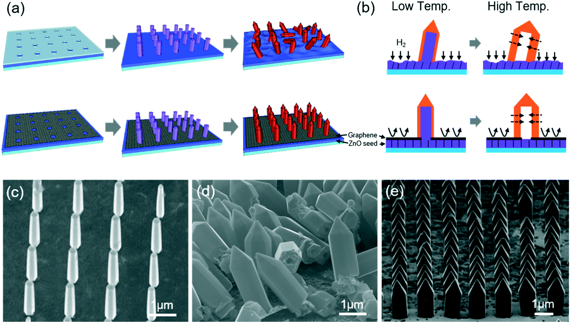 | ||
| Fig. 1 (a) Schematics illustrating the growth of GaN crystals on a ZnO rod array: (top) collapsed GaN crystals grown on a ZnO rod array on a bare ZnO seed layer. (bottom) Vertically-aligned GaN crystal array grown on a ZnO rod array on a ZnO seed layer via holes in the graphene mask. (b) Schematic side view images illustrating the two-step GaN crystal growth on ZnO rod arrays. (c) SEM images of a typical ZnO rod array, (d) collapsed GaN crystals, and (e) a vertically-aligned GaN crystal array. | ||
To demonstrate that this approach can be used to achieve complicated 3D GaN structures, we investigated the GaN crystal growth behavior for different types of ZnO templates and GaN growth conditions. When the GaN shell growth occurred on vertically-grown ZnO hexagonal rod (h-rod) arrays at a relatively high temperature of 1000 °C, the resulting GaN crystals generally had a pencil-like morphology consisting of (i) the lower part of the h-pillar and (ii) the upper part of the h-pyramid (Fig. 1e); the pillars and pyramids were terminated with the very smooth planes of (1![[1 with combining macron]](https://www.rsc.org/images/entities/char_0031_0304.gif) 00) and (101), respectively. When the ZnO templates were changed from thinner rods to thicker and/or shorter rods, the portions of the h-pillars of GaN crystals became smaller, resulting in a morphology similar to the h-tent morphology (left and middle panels of Fig. 2a and d). Interestingly, while the height of the h-pyramid (Hpyr) gradually increased with increases in the radius of the h-pillar (Rpil) up to 0.45 μm; Hpyr became saturated and remained unchanged (Hpyr = ∼0.8 μm) as Rpil increased further (right panel of Fig. 2a and b, blue dots and dashed lines). Meanwhile, the height of the h-pillars (Hpyr) remained comparable to the height of the ZnO h-rods, regardless of Rpil. Overall, the tips changed from pyramid-shaped to truncated hexagonal prism-shaped crystals terminated with rough hexa-planes (Fig. 2c, upper panels). The angle between the tilted dashed lines and the x-axis was 62° (Fig. 2b), which is comparable to that between the side (101) plane and the (000) basal plane.35
00) and (101), respectively. When the ZnO templates were changed from thinner rods to thicker and/or shorter rods, the portions of the h-pillars of GaN crystals became smaller, resulting in a morphology similar to the h-tent morphology (left and middle panels of Fig. 2a and d). Interestingly, while the height of the h-pyramid (Hpyr) gradually increased with increases in the radius of the h-pillar (Rpil) up to 0.45 μm; Hpyr became saturated and remained unchanged (Hpyr = ∼0.8 μm) as Rpil increased further (right panel of Fig. 2a and b, blue dots and dashed lines). Meanwhile, the height of the h-pillars (Hpyr) remained comparable to the height of the ZnO h-rods, regardless of Rpil. Overall, the tips changed from pyramid-shaped to truncated hexagonal prism-shaped crystals terminated with rough hexa-planes (Fig. 2c, upper panels). The angle between the tilted dashed lines and the x-axis was 62° (Fig. 2b), which is comparable to that between the side (101) plane and the (000) basal plane.35
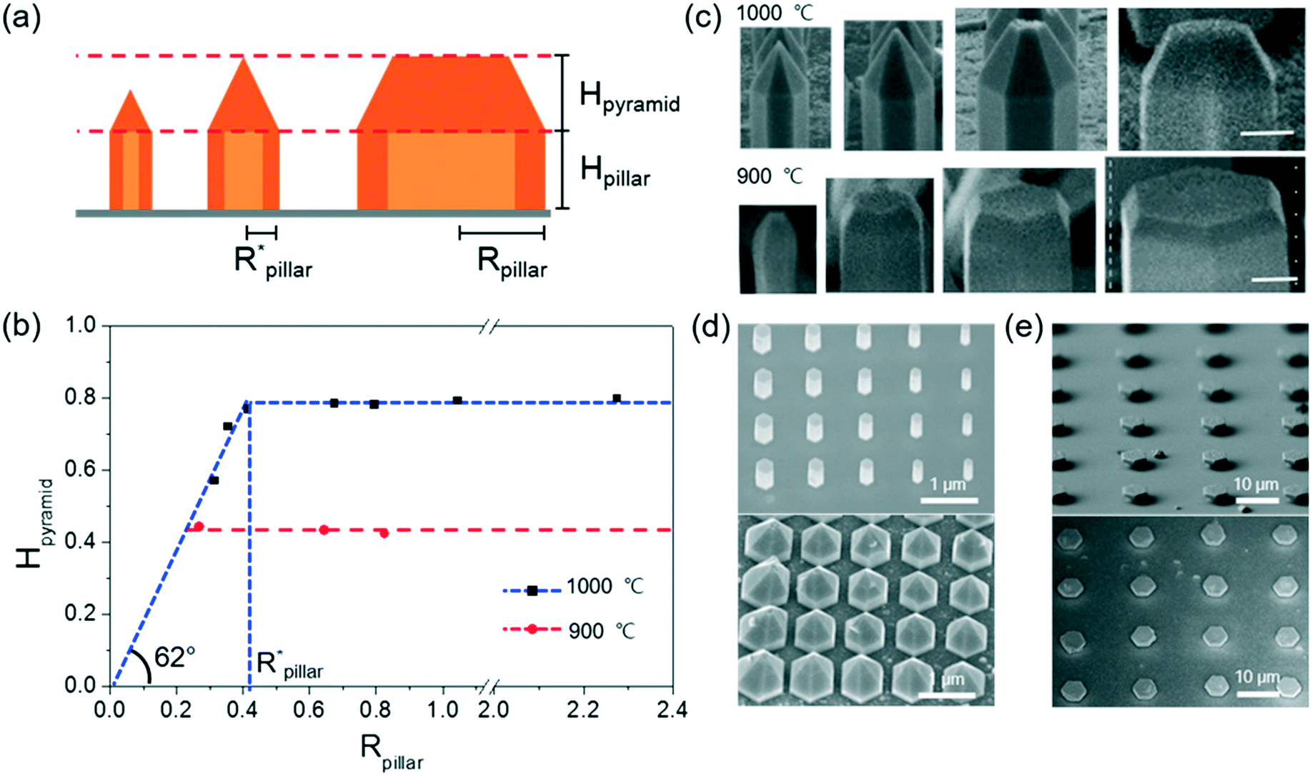 | ||
| Fig. 2 Growth of various types of 3D GaN crystals. (a) Schematics illustrating the exterior morphologies of GaN crystals for various Rpillar values. (b) Hpyramidversus Rpillar plots of GaN crystals. (c) SEM images of GaN crystals with increasing Rpillar grown at 1000 °C (upper panels) and 900 °C (lower panels). (d) h-Tent shaped GaN crystals (bottom) grown epitaxially on ZnO rods (top). (e) h-Plate shaped GaN crystals (bottom) grown on ZnO plates (top). | ||
On the other hand, changes in the growth conditions, i.e., the growth temperature or source concentration, also affected the GaN crystal morphology. We found that as the growth temperature decreased, the height of the pyramid (Htip) decreased. The saturated Hpyr values were ∼0.43 μm at 900 °C (Fig. 2b, red dots and dashed lines, Fig. 2c, lower panels), which was roughly half of the value at 1000 °C. Furthermore, GaN growth at 900 °C on the template with laterally-grown ZnO plates, which was achieved by controlling the polarity-selective crystal growth direction,26 produced an array of GaN micro-crystals with a dominant and flat (0001) surface (Fig. 2e).
The observed temperature-sensitive morphology change might be due to a correlation between the desorption rate and the absorption rate of Ga adatoms at various temperatures depending on the plane, i.e., the (0001) and (101) planes of the GaN crystal. Basically, the height of the pyramid increases as the absorption rate increases relative to the desorption rate on the (0001) surface. The opposite phenomenon occurs for the (101) surface. In general, the growth rate on the (101) plane of the GaN crystal is relatively lower than that on the (0001) plane because the (101) plane is energetically more stable than the (0001) plane. This results in the formation of an upper h-pyramid (or truncated h-prism), even on the ZnO h-rod templates. On the other hand, the ratio of the desorption rate to the absorption rate of Ga adatoms increases with increasing temperature, but the ratio on the (101) surface increases more rapidly with temperature than that on the (0001) surface, producing higher tips at higher temperatures.36–38
We performed transmission electron microscopy (TEM) analysis to investigate the crystallinity of the 3D GaN structure on a crystal that was vertically cross-sectioned by focused ion beam (FIB) milling. The hollow structure of the 3D GaN crystal, which has an inner void where the ZnO hexaplate-shaped template was located, was observed in a low-magnification TEM image (Fig. 3a). Note that the particles found in the void region (marked by an arrow/dashed line in Fig. 3a) are by-products of FIB milling, as confirmed by energy-dispersive X-ray spectroscopy (EDS) analysis (Fig. S2†). Fig. 3b shows the selected area diffraction (SAED) patterns along the <0001> zone axis obtained at the positions marked [I] in Fig. 3a. The SAED pattern and fast Fourier transform (FFT) patterns measured at different positions in the same crystals are an exact match, indicating a crystallographically identical orientation and structure (insets of Fig. 3c and d). In addition, high-resolution TEM (HR-TEM) images clearly show the lattice fringes with a d-spacing of 0.52 nm, corresponding to the (0001) plane of wurtzite GaN (Fig. 3b and c).39 The TEM results confirmed that nearly single crystalline and high-quality GaN layers were epitaxially grown on ZnO crystals that eventually disappeared during GaN growth. Using this TEM analysis, we confirmed that the 3D GaN grew as a single crystal both internally and at the top surface.
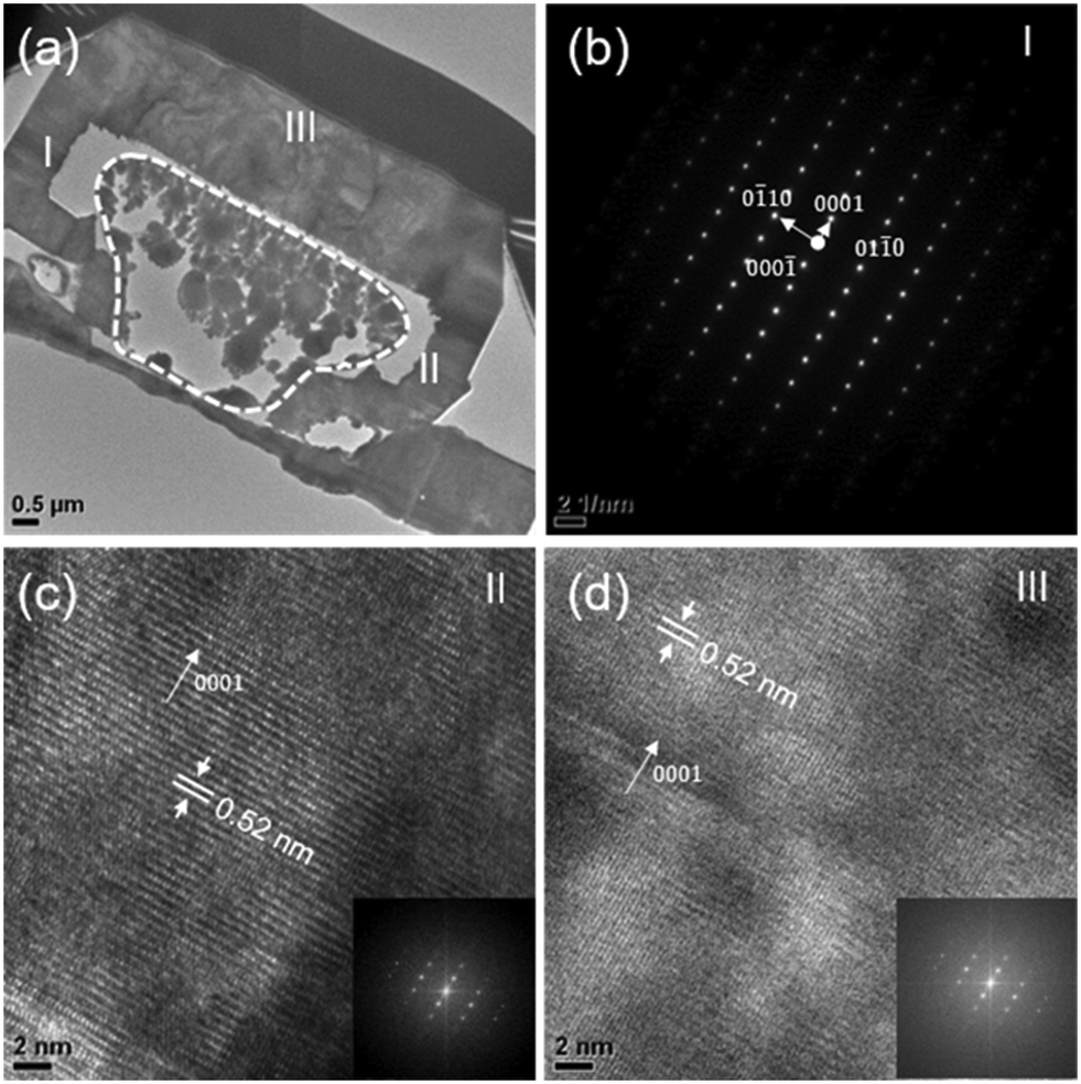 | ||
| Fig. 3 Microstructural analysis of 3D GaN. (a) Low magnification TEM image of a vertically cross-sectioned GaN crystal (top left). (b) SAED pattern obtained at the positions marked [I]. (c and d) HR-TEM images taken from the regions marked [II] and [III] in (a), along with the corresponding FFT images (insets). | ||
We further established n-type and p-type doping in the GaN crystals, as well as fabricated μ-LED arrays consisting of 8 μm diameter GaN crystals, schematically shown in Fig. 4a. Bottom n-contact and top p-contact electrodes of the LEDs were made with graphene and a Ni/Au metal layer, respectively, followed by rapid thermal annealing at 300 °C to achieve ohmic contacts. Polyimide (PI) filled the spacing between the GaN crystals and partially etched with O2 plasma until the top portions of the GaN crystals were exposed, thereby eliminating the current leakage between the two electrodes. Optical microscopy images in Fig. 4b showed blue emission from the 3 × 3 array of p–n junction GaN crystals when forward currents of 0.17, 0.56, and 0.88 mA were applied to the devices (Fig. 4b). Note that the pixels on the bottom row were shaded with the probing tip, as marked by the dotted line. The light emission is strong enough to be seen with the unaided eye. Plots of the current and electroluminescence (EL) intensity versus applied voltage exhibit a typical rectifying transport behavior, and the emission intensity increases in proportion to the current (Fig. 4c). In addition, the EL spectra show dominant blue emission peaks centered at 450 nm (Fig. 4d). A red shift in emission peaks compared with the near band edge emission in n-type GaN was also observed in photoluminescence measurements (inset of Fig. 4d and S3†). Similar results were also observed in heavily Mg-doped p-GaN thin films and planar p–n GaN LEDs.40,41 This was attributed to a donor–acceptor pair recombination involving a sharp transition from localized states to delocalized states occurring within an Urbach tail.41
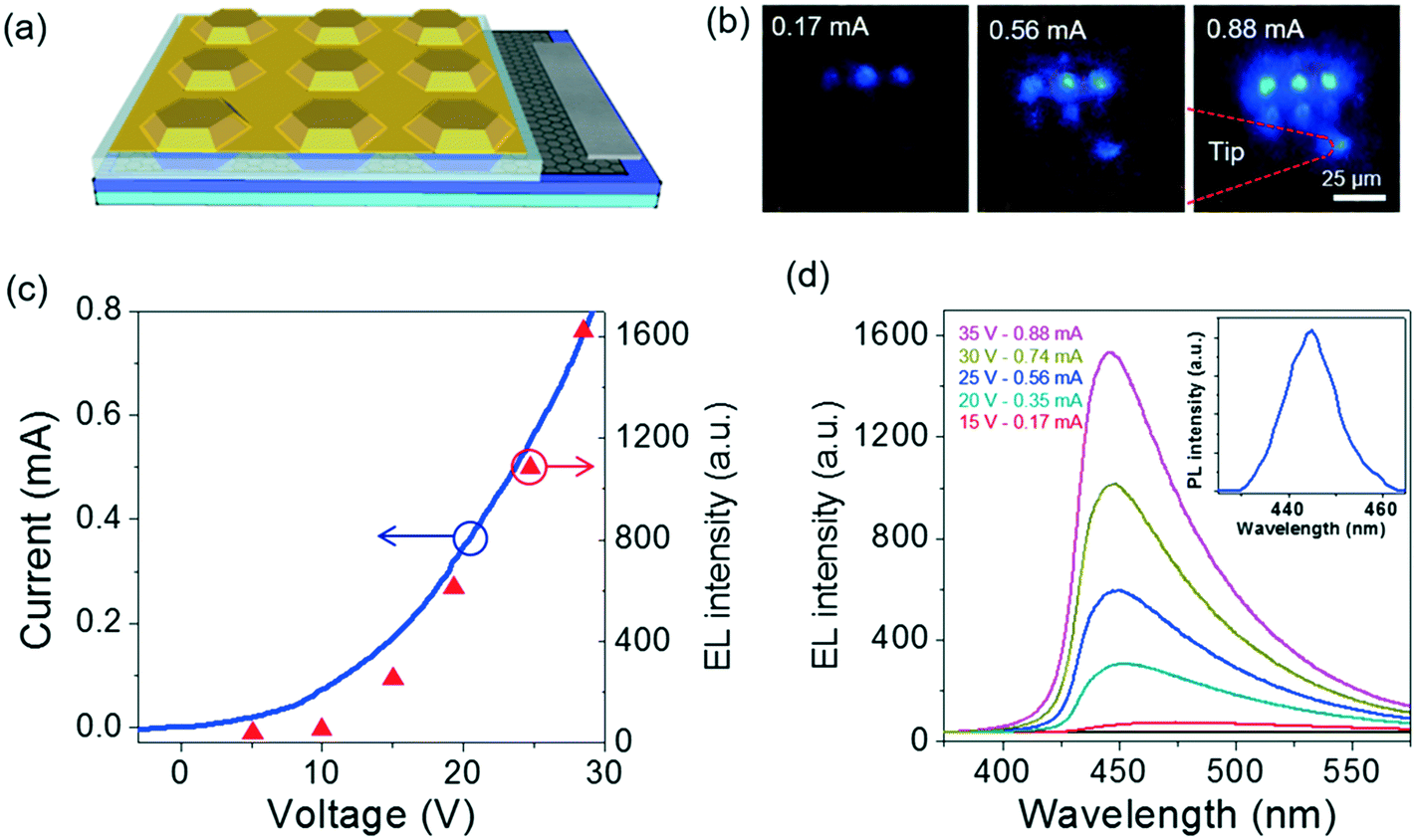 | ||
| Fig. 4 3D GaN p–n junction LED. (a) Schematic image of 3D GaN LEDs. (b) OM images of the current-dependent light emission from a 3 × 3 μ-LED array. (c) Current and EL intensity versus voltage plots. (d) EL spectra of 3D GaN LED measured at various voltages and a PL spectrum from the same crystals (inset). | ||
Conclusions
In conclusion, we demonstrated MOVPE growth of 3D GaN microcrystals on morphology and position-controlled ZnO templates. During epitaxial growth, the graphene mask layer prevented damage of the supporting ZnO seed layers, thereby enabling the growth of well-aligned GaN crystals. In addition, we found that the morphology of GaN crystals, especially the tips, is determined by temperature-sensitive Ga adatom–surface interactions. This feature, together with the use of various types of ZnO templates, facilitated fine control of the crystal exterior morphology from h-pencil to h-tent, then to h-plate. Structural analyses based on TEM also confirmed the single crystalline nature of these GaN crystals. Furthermore, we observed blue light emission from the p–n junction GaN crystal array, suggesting that this may be a new way to fabricate more-complicated 3D light emitting crystals. We believe that the LED performance can be further improved by introducing InGaN-based quantum well structures and a transparent ohmic contact electrode to the top p-GaN layer. The resulting μ-LED arrays based on 3D GaN/InxGa1−xN structures should provide new functionalities, such as wavelength tuning and/or multiplexing, piezo-photo-electricity, and extraordinary light extraction or confinement.Acknowledgements
This work was supported by the National Research Foundation of Korea (NRF) funded by the Ministry of science, ICT and Future Planning (MSIP) (No. 2015R1A2A2A11001426, No. 2016K1A4A3914691). G.-C. Y. acknowledges support by the Global Research Laboratory Program (2015K1A1A2033332) through the NRF funded by the MSIP.References
- L. M. Tong, R. R. Gattass, J. B. Ashcom, S. L. He, J. Y. Lou, M. Y. Shen, I. Maxwell and E. Mazur, Nature, 2003, 426, 816–819 CrossRef CAS PubMed
.
- S. Noda, K. Tomoda, N. Yamamoto and A. Chutinan, Science, 2000, 289, 604–606 CrossRef CAS PubMed
- X. Q. Huang, Y. Lai, Z. H. Hang, H. H. Zheng and C. T. Chan, Nat. Mater., 2011, 10, 582–586 CrossRef CAS PubMed
- W. Cai, U. K. Chettiar, A. V. Kildishev and V. M. Shalaev, Nat. Photonics, 2007, 1, 224–227 CrossRef CAS
- Z. L. Lu, S. Y. Shi, C. A. Schuetz, J. A. Murakowski and D. W. Prather, Opt. Express, 2005, 13, 5592–5599 Search PubMed
- S. Jeon, J. U. Park, R. Cirelli, S. Yang, C. E. Heitzman, P. V. Braun, P. J. Kenis and J. A. Rogers, Proc. Natl. Acad. Sci. U. S. A., 2004, 101, 12428–12433 CrossRef CAS PubMed
- T. A. Schaedler, A. J. Jacobsen, A. Torrents, A. E. Sorensen, J. Lian, J. R. Greer, L. Valdevit and W. B. Carter, Science, 2011, 334, 962–965 CrossRef CAS PubMed
- L. Sun, S. T. Parker, D. Syoji, X. Wang, J. A. Lewis and D. L. Kaplan, Adv. Healthcare Mater., 2012, 1, 729–735 CrossRef CAS PubMed
- D. Therriault, R. F. Shepherd, S. R. White and J. A. Lewis, Adv. Mater., 2005, 17, 395–399 CrossRef CAS
- A. J. Wang, S.-L. Chen, P. Dong, C. T. Hu and L. Sang, Thin Solid Films, 2011, 519, 1798–1802 CrossRef CAS
- M. Deubel, G. von Freymann, M. Wegener, S. Pereira, K. Busch and C. M. Soukoulis, Nat. Mater., 2004, 3, 444–447 CrossRef CAS PubMed
- S. Shoji and S. Kawata, Appl. Phys. Lett., 2000, 76, 2668–2670 CrossRef CAS
- E. C. Nelson, N. L. Dias, K. P. Bassett, S. N. Dunham, V. Verma, M. Miyake, P. Wiltzius, J. A. Rogers, J. J. Coleman, X. Li and P. V. Braun, Nat. Mater., 2011, 10, 676–681 CrossRef CAS PubMed
- K. Chung, H. Beak, Y. Tchoe, H. Oh, H. Yoo, M. Kim and G.-C. Yi, APL Mater., 2014, 2, 092512 CrossRef
- W. I. Park and G. C. Yi, Adv. Mater., 2004, 16, 87–90 CrossRef CAS
- X. Wang, S. Li, S. Fündling, J. Wei, M. Erenburg, H.-H. Wehmann, A. Waag, W. Bergbauer, M. Strassburg, U. Jahn and H. Riechert, Cryst. Growth Des., 2012, 12, 2552–2556 CAS
- Y. H. Ko, J. H. Kim, L. H. Jin, S. M. Ko, B. J. Kwon, J. Kim, T. Kim and Y. H. Cho, Adv. Mater., 2011, 23, 5364–5369 CrossRef CAS PubMed
- K. Chung, H. Yoo, J. K. Hyun, H. Oh, Y. Tchoe, K. Lee, H. Baek, M. Kim and G. C. Yi, Adv. Mater., 2016, 28, 7688–7694 CrossRef CAS PubMed
- Y. J. Hong, C. H. Lee, A. Yoon, M. Kim, H. K. Seong, H. J. Chung, C. Sone, Y. J. Park and G. C. Yi, Adv. Mater., 2011, 23, 3284–3288 CrossRef CAS PubMed
- S.-H. Lim, Y.-H. Ko, C. Rodriguez, S.-H. Gong and Y.-H. Cho, Light: Sci. Appl., 2016, 5, e16030 CrossRef CAS
- K. Chung, C. H. Lee and G. C. Yi, Science, 2010, 330, 655–657 CrossRef CAS PubMed
- C.-H. Lee, J. Yoo, Y. J. Hong, J. Cho, Y.-J. Kim, S.-R. Jeon, J. H. Baek and G.-C. Yi, Appl. Phys. Lett., 2009, 94, 213101 CrossRef
- Y. Tchoe, C. H. Lee, J. B. Park, H. Baek, K. Chung, J. Jo, M. Kim and G. C. Yi, ACS Nano, 2016, 10, 3114–3120 CrossRef CAS PubMed
- S. B. Kim, S. Kim, S. S. Kwon, W. W. Lee, J.-S. Kim, W. I. Park and G. Brennecka, J. Am. Ceram. Soc., 2013, 96, 3500–3503 CrossRef CAS
- J. M. Lee, Y. S. No, S. Kim, H. G. Park and W. I. Park, Nat. Commun., 2015, 6, 6325 CrossRef CAS PubMed
- W. W. Lee, S. Chang, D. W. Yang, J. M. Lee, H.-G. Park and W. I. Park, CrystEngComm, 2016, 18, 8262–8269 RSC
- W. W. Lee, J. Yi, S. B. Kim, Y.-H. Kim, H.-G. Park and W. I. Park, Cryst. Growth Des., 2011, 11, 4927–4932 CAS
- K. T. Park, F. Xia, S. W. Kim, S. B. Kim, T. Song, U. Paik and W. I. Park, J. Phys. Chem. C, 2013, 117, 1037–1043 CAS
- H. Zhang, D. R. Yang, D. S. Li, X. Y. Ma, S. Z. Li and D. L. Que, Cryst. Growth Des., 2005, 5, 547–550 CAS
- J.-H. Kim, C.-S. Oh, Y.-H. Ko, S.-M. Ko, K.-Y. Park, M. Jeong, J. Y. Lee and Y.-H. Cho, Cryst. Growth Des., 2012, 12, 1292–1298 CAS
- W. W. Lee, S. B. Kim, J. Yi, W. T. Nichols and W. I. Park, J. Phys. Chem. C, 2012, 116, 456–460 CAS
- J. M. Lee, H. Y. Jeong and W. Il Park, J. Electron. Mater., 2010, 39, 2190–2195 CrossRef CAS
- Y.-J. Kim, W. W. Lee, I.-C. Choi, B.-G. Yoo, S. M. Han, H.-G. Park, W. I. Park and J.-I. Jang, Acta Mater., 2013, 61, 7180–7188 CrossRef CAS
- K. S. Novoselov, V. I. Fal'ko, L. Colombo, P. R. Gellert, M. G. Schwab and K. Kim, Nature, 2012, 490, 192–200 CrossRef CAS PubMed
- T. Song, J. W. Choung, J.-G. Park, W. I. Park, J. A. Rogers and U. Paik, Adv. Mater., 2008, 20, 4464–4469 CrossRef CAS
- B. O. Jung, S.-Y. Bae, Y. Kato, M. Imura, D.-S. Lee, Y. Honda and H. Amano, CrystEngComm, 2014, 16, 2273 RSC
- S. Kitamura, K. Hiramatsu and N. Sawaki, Jpn. J. Appl. Phys., Part 2, 1995, 34, L1184–L1186 CrossRef CAS
- A. Lundskog, C. W. Hsu, D. Nilsson, K. F. Karlsson, U. Forsberg, P. O. Holtz and E. Janzén, J. Cryst. Growth, 2013, 363, 287–293 CrossRef CAS
- S. D. Hersee, X. Y. Sun and X. Wang, Nano Lett., 2006, 6, 1808–1811 CrossRef CAS PubMed
- S. Nakamura, T. Mukai and M. Senoh, Jpn. J. Appl. Phys., Part 2, 1991, 30, L1998–L2001 CrossRef CAS
- J. S. Colton and P. Y. Yu, Appl. Phys. Lett., 2001, 78, 2500–2502 CrossRef CAS
Footnote |
| † Electronic supplementary information (ESI) available. See DOI: 10.1039/c7ce00057j |
| This journal is © The Royal Society of Chemistry 2017 |