
Compositionally controlled band gap and photoluminescence of ZnSSe nanofibers by electrospinning†
Lin-Jer
Chen
*a,
Chia-Rong
Lee
*a,
Yu-Ju
Chuang
b,
Zhao-Han
Wu
b and
Chienyi
Chen
c
aDepartment of Photonics, National Cheng Kung University, Tainan, Taiwan. E-mail: linjerchen@hotmail.com; crlee@mail.ncku.edu.tw
bDepartment of Materials Science and Engineering, National Cheng Kung University, Tainan, Taiwan
cDepartment of Chemistry, National Cheng Kung University, Tainan, Taiwan
First published on 1st May 2015
Abstract
A simple, non-toxic, low-priced, and reproducible manipulation, which meets the standards of green chemistry, is introduced for the synthesis of ZnSxSe1−x nanofibers. ZnSxSe1−x nanofibers have been prepared in the entire composition range from ZnSe to ZnS by using a low-cost wet-chemical method. The effects of polymer (PVB) concentrations, reactant (S/Se) concentrations and reaction conditions (applied voltage, viscosity, and work distance) have been investigated. We have demonstrated that wurtzite ZnSxSe1−x showing a fiber-like morphology can be kinetically stabilized in the presence of an electrospinning system.
One-dimensional (1D) semiconductor nanomaterials have received much attention for their unique electronic, optical, physical and chemical properties, and potential applications in optoelectronic devices, photonics, energy conversion, catalysis and biosensors.1–3 Amid the group II–VI semiconductors, ZnSSe, as a direct band gap material with a bulk band gap of 2.70–3.5 eV, is considered as a good candidate for light-emitting devices and other optoelectronic devices.4,5 Band gaps are one of the most significant factors in considering semiconductor materials for optoelectronic applications since they resolve the spectral characteristics of absorption and emission processes. Nanofibers open a new sight of band gaps through alloying with nearly assertive compositions.6–8 ZnSe (bulk band gap 2.7 eV) and ZnS (bulk band gap 3.6 eV) are wide band gap semiconductor materials. These wide band gap semiconductors are also appealing hosts for the formation of doped nanomaterials.9,10 For these reasons, synthesis of high-quality ZnSe and ZnS nanomaterials is still an attractive topic.10–16
An important region in nanotechnology is the fabrication of composite structures containing different semiconductor nanocrystals. In semiconductor nanomaterials, band gap energy can easily be handled by slight tuning of their composition and size. Surface morphology also plays an important function in determining the properties of the system, especially on the nanoscale because of their large surface-to-volume ratio. Concomitant control of the morphology and structure of semiconductor nanomaterials provides chances to tune and research their optical properties. The properties of materials change dramatically with size and composition, which comprises thermodynamic stability. Also, structural transformations have been demonstrated to occur in nanoscale materials at lower temperatures.17
As one of the important Zn-based II–VI semiconductors, ZnSxSe1−x has been intended to be a suitable material for photoelectronic devices due to its wide direct band gap and high photoresistivity.18–20 Moreover, ZnSxSe1−x is also a promising material for windows, biomedical labels, output couplers, lenses, and optically controlled switches, due to its low absorptivity at infrared wavelength and exciton binding energy. Research efforts in the field of optical control of ZnSxSe1−x have been mostly focused on fabricating 1D nanofibers by an easy electrospinning process (as shown in Fig. S1†). In the present study, we report the synthesis of ZnSxSe1−x in the wurtzite phase at low temperature in the presence of PVB under annealing conditions. ZnSxSe1−x nanofibers were prepared by electrospinning of a mixture of selenium and sulfur precursors into the zinc precursor based on previously reported methods (please see the ESI† for experimental details).3,21–23 The phase and morphology evolutions of ZnSxSe1−x in the presence of PVB are systematically studied by scanning electron microscopy (SEM), transmission electron microscopy (TEM), X-ray diffraction (XRD), X-ray photoelectron spectroscopy (XPS), and UV–visible spectroscopy, as well as by using a diode pumped solid state laser (DPSS).
The influence of the parameters of the solution on the morphology of the nanofibers was studied. The diameters of PVB/ZnSxSe1−x composite fibers obtained at different work distances and concentrations are shown in Fig. 1a. With increasing concentration ratio, the diameter of PVB/ZnSxSe1−x composite fibers decreased and beads-on-a-string structures appeared. When the concentration ratio was increased, the beads on the fibers decreased, as shown in Fig. 1a (cubic). In contrast with various concentrations, the capping medium forms stable complexes with the precursor, in which rapid formation of small nanoparticles as the crystal nuclei and slow crystal growth to form nanofibers from the crystal nuclei according to the inherent crystal structure occur. In this case, the work distance from the tip of the needle to the collector is long enough for elongation and solidification of the jet to form fibers, as shown in Fig. 1a (triangle). However, when the work distance was reduced, the fiber diameter increased. That is, the morphology of the electrospun structure transformed rapidly and the evaporation of solvent in the jet was somewhat suppressed. The lashing instability, which facilitated the diffusion of the jet, was extremely suppressed.24 The results show that a large work distance is preferred for electrospinning.
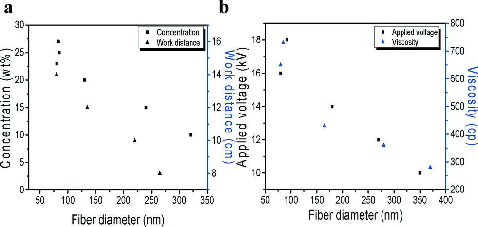 | ||
| Fig. 1 (a) Diameters of PVB/ZnS0.5Se0.5 composite fibers for various concentration ratios and work distances. (b) Diameters of PVB/ZnS0.5Se0.5 composite fibers for various viscosities and applied voltages. | ||
Fig. 1b shows the fiber diameters of PVB/ZnSxSe1−x composite fibers for various viscosities and applied voltages (10 kV, 15 kV, 20 kV, and 22 kV). The fiber diameter decreased with increasing viscosity, as expected (Fig. 1b, triangle). One hundred PVB/ZnSxSe1−x composite fibers were selected from ten spots of 60 × 60 μm2 to measure the distribution of the diameters. This may be due to the more expanded conformation of PVB/ZnSxSe1−x in the solution caused by electrostatic repulsion between molecules in the PVB/ZnSxSe1−x mixture. The molecular entanglement of PVB/ZnSxSe1−x in solution is thus expected to be higher. It was observed that the diameter distribution of the PVB/ZnSxSe1−x composite fibers decreased with increasing applied voltage (Fig. 1b, cubic). The jet is driven by a high electrical potential applied between the collector and the solution. The electrical forces which stretch the wires are resisted by the elongational viscosity of the jet. A reduction in size with applied voltage has been reported for various electrospun organic fibers.25
Fig. 2 shows a series of SEM images of PVB/ZnSxSe1−x nanofibers obtained from precursor solutions with concentration ratios of 5 wt.%, 10 wt.%, 20 wt.%, 23 wt.%, and 27 wt.% (PVB/ethanol content ratio). As can be seen in Fig. 2a, fewer fibers were obtained when the ratio was 5 wt.%. Because of the decrease in the ratio, the conductivity of the fibers increased, the viscosity of the fibers decreased, and beads-on-a-string structures appeared. When the ratio was further increased, the beads on the fibers decreased. The results presented that these fibers preferred generated at the high concentration. A high conductivity solvent is beneficial to ion diffusion and reduces resistance, whereas a high viscosity solvent can make the diffusion of ions difficult to achieve, thus reducing conductivity.26 When the concentration of PVB was increased, beads-on-a-string structures were observed, as shown in Fig. 2b–d, and the bead density decreased. PVB/ZnSxSe1−x nanofibers with smooth surfaces were obtained when the PVB/ethanol ratio was 23 wt.%. The concentration of PVB is accordingly a key factor in the preparation of smooth PVB/ZnSxSe1−x nanofibers. PVB acted as the capping medium, whereas the states by which the PVB/ZnSxSe1−x composite nanofibers exist are adsorbed polymer chains that induce not only steric repulsion but also bridging attraction. Pure PVB fibers are shown in Fig. 2f; their morphological surface is smoother than that of PVB/ZnSxSe1−x fibers. Fig. S2† shows the TGA thermogram of the PVB/ZnSxSe1−x nanofibers. It was observed that the weight essentially decreases in the low temperature region. The higher thermal stability of PVB/ZnSxSe1−x fibers might be attributed to their higher chain compactness due to the interaction between the PVB and ZnSxSe1−x materials.27–29 It is clear from the TG curve that all PVB and organic groups were removed completely at 680 °C, resulting in a metal oxide composite phase.30
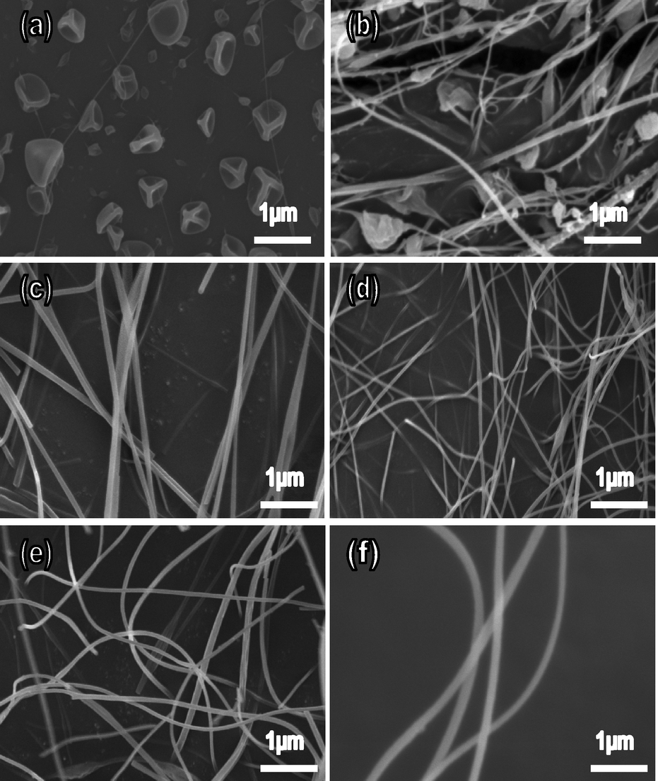 | ||
| Fig. 2 SEM images of PVB/ZnS0.5Se0.5 composite nanofibers electrospun from (a) 5 wt.%, (b) 10 wt.%, (c) 20 wt.%, (d) 23 wt.%, and (e) 27 wt.% aqueous solutions at 16 kV, and (f) pure PVB fibers. | ||
ZnS and ZnSe have been known to crystallize with both cubic (zinc-blende) and wurtzite (hexagonal) structures.31 For this purpose, it is important to prove the crystal structure of the synthesized nanofibers. The phase recognition was carried out by X-ray diffraction (XRD) as shown in Fig. 3a. The average crystal domain size of the nanocrystals calculated using Scherrer's equation based on the (100) peak is 75 nm (D = Kλ/(β![[thin space (1/6-em)]](https://www.rsc.org/images/entities/char_2009.gif) cosθ); K = 0.89, λ = 0.15418 nm, β = FWHM, θ = diffraction angle). The major diffraction peaks of zinc sulfide (zinc selenium) observed at 2θ = 26.9, 28.5, 30.52, 39.61, 47.56, 51.77, 55.5, and 56.39° (2θ = 25.86, 27.39, 29.3, 38.03, 45.61, 49.64, 53.18, and 54.03°) can be indexed to the (100), (002), (101), (102), (110), (103), (200), and (112) peaks of the wurtzite (hexagonal) crystal structure, respectively. Then, in order to determine whether the nanocrystals are hexagonal, it is crucial to observe the minor peaks that are unique to the hexagonal structure. For example, the minor peaks at 55.5°, 57.5°, and 63.5° (53.18°, 55.16°, and 60.85°) corresponding to the (200), (201), and (202) peaks, respectively, are unique to the hexagonal structure (JCPDS 36-1450 and 80-0008) and are shown in Fig. 3a. The ZnSxSe1−x nanocrystal diffraction peaks also show patterns gradually shifting toward a lower angle with decreasing sulfide content, due to the decreased lattice spacing with smaller sulfide atoms substituting for larger selenium atoms (Fig. S3†). A similar behavior could be found in the literature.32,33 The morphology of ZnS0.5Se0.5 nanofibers was characterized using a transmission electron microscope (H-800) with an accelerating voltage of 160 kV. Fig. 3b shows the TEM image of ZnS0.5Se0.5 nanofibers electrospun at 16 kV. The fiber-like nanostructures have diameters from 70 to 80 nm and lengths from hundreds of nanometers to several micrometers. By changing the reaction concentration, viscosity, collector distance, and applied voltage, the nanofiber size can be easily controlled. When the PVB/ethanol ratio was increased from 10 wt.% to 27 wt.% with a tip-to-collector distance of 14 cm, the diameter decreased to about 75 nm. The growth directions of the nanofibers were determined from the selected area electron diffraction (SAED) patterns shown in the inset of Fig. 3c. A high-resolution bright-field TEM image of characteristic nanofibers from wurtzite synthesis is shown in Fig. 3c. The image is taken along the [01
cosθ); K = 0.89, λ = 0.15418 nm, β = FWHM, θ = diffraction angle). The major diffraction peaks of zinc sulfide (zinc selenium) observed at 2θ = 26.9, 28.5, 30.52, 39.61, 47.56, 51.77, 55.5, and 56.39° (2θ = 25.86, 27.39, 29.3, 38.03, 45.61, 49.64, 53.18, and 54.03°) can be indexed to the (100), (002), (101), (102), (110), (103), (200), and (112) peaks of the wurtzite (hexagonal) crystal structure, respectively. Then, in order to determine whether the nanocrystals are hexagonal, it is crucial to observe the minor peaks that are unique to the hexagonal structure. For example, the minor peaks at 55.5°, 57.5°, and 63.5° (53.18°, 55.16°, and 60.85°) corresponding to the (200), (201), and (202) peaks, respectively, are unique to the hexagonal structure (JCPDS 36-1450 and 80-0008) and are shown in Fig. 3a. The ZnSxSe1−x nanocrystal diffraction peaks also show patterns gradually shifting toward a lower angle with decreasing sulfide content, due to the decreased lattice spacing with smaller sulfide atoms substituting for larger selenium atoms (Fig. S3†). A similar behavior could be found in the literature.32,33 The morphology of ZnS0.5Se0.5 nanofibers was characterized using a transmission electron microscope (H-800) with an accelerating voltage of 160 kV. Fig. 3b shows the TEM image of ZnS0.5Se0.5 nanofibers electrospun at 16 kV. The fiber-like nanostructures have diameters from 70 to 80 nm and lengths from hundreds of nanometers to several micrometers. By changing the reaction concentration, viscosity, collector distance, and applied voltage, the nanofiber size can be easily controlled. When the PVB/ethanol ratio was increased from 10 wt.% to 27 wt.% with a tip-to-collector distance of 14 cm, the diameter decreased to about 75 nm. The growth directions of the nanofibers were determined from the selected area electron diffraction (SAED) patterns shown in the inset of Fig. 3c. A high-resolution bright-field TEM image of characteristic nanofibers from wurtzite synthesis is shown in Fig. 3c. The image is taken along the [01![[1 with combining macron]](https://www.rsc.org/images/entities/char_0031_0304.gif) 0] zone axis with the (220), (204), and (024) crystallographic planes indicated by white lines. Spacing measurements based on 6 planes indicated d-spacings of 2.94 ± 0.02 Å for the (220) plane and 3.12 ± 0.02 Å for the (204) and (024) planes. The measured angle between the (220) and (024) planes is 56.5 ± 0.5° and that between (204) and (024) planes is 62 ± 0.5°. If the structure were cubic, the measured angles should be 60° between all three planes, and the measured d-spacings should be 3.12 Å. These observed differences provide additional evidence of lattice distortion that results from cation ordering and the wurtzite crystal structure. The zone axis of the SAED pattern was determined to be [0001], and the pattern is typical for nanocrystals obtained with a similar synthesis process. These extra spots correspond to 2/3 the distance of the (114) or (122) fundamental reflections and have a d-spacing of 3.1 Å. Both high-resolution TEM (Fig. 3b) and XRD (Fig. 3a) confirmed that the nanocrystals are crystalline with a hexagonal wurtzite structure. No other crystal phases were observed in the XRD patterns of the product. Compositional analysis by XPS and quantum yields showed that the nanocrystals in the sample has a molar Zn/Se/S ratio of 1:x:1 − x (x = 0, 0.2, 0.5, 0.8 and 1) and the composition of individual particles measured by EDS was 1:x:1 − x with a variation from particle to particle less than the experimental error of ca. ±2 atom% (see Table S1 and Fig. S4†).
0] zone axis with the (220), (204), and (024) crystallographic planes indicated by white lines. Spacing measurements based on 6 planes indicated d-spacings of 2.94 ± 0.02 Å for the (220) plane and 3.12 ± 0.02 Å for the (204) and (024) planes. The measured angle between the (220) and (024) planes is 56.5 ± 0.5° and that between (204) and (024) planes is 62 ± 0.5°. If the structure were cubic, the measured angles should be 60° between all three planes, and the measured d-spacings should be 3.12 Å. These observed differences provide additional evidence of lattice distortion that results from cation ordering and the wurtzite crystal structure. The zone axis of the SAED pattern was determined to be [0001], and the pattern is typical for nanocrystals obtained with a similar synthesis process. These extra spots correspond to 2/3 the distance of the (114) or (122) fundamental reflections and have a d-spacing of 3.1 Å. Both high-resolution TEM (Fig. 3b) and XRD (Fig. 3a) confirmed that the nanocrystals are crystalline with a hexagonal wurtzite structure. No other crystal phases were observed in the XRD patterns of the product. Compositional analysis by XPS and quantum yields showed that the nanocrystals in the sample has a molar Zn/Se/S ratio of 1:x:1 − x (x = 0, 0.2, 0.5, 0.8 and 1) and the composition of individual particles measured by EDS was 1:x:1 − x with a variation from particle to particle less than the experimental error of ca. ±2 atom% (see Table S1 and Fig. S4†).
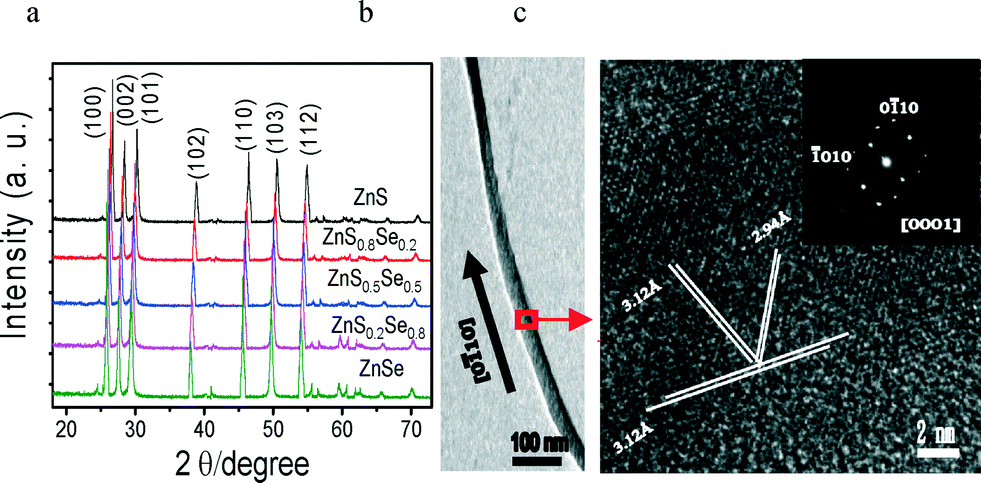 | ||
| Fig. 3 (a) X-ray diffraction patterns of as-synthesized ZuSxSe1−x nanofibers at different values of S/Se ratio as a function of x = 0, 0.2, 0.5, 0.8 and 1. (b) High-resolution TEM of wire-like ZnS0.5Se0.5 nanostructure recorded along [0001] and (c) TEM images of as-synthesized ZnS0.5Se0.5 nanofibers and their SAED pattern (inset). | ||
The purity and composition of synthesized ZnSSe were examined by XPS analyses. The typical XPS results are shown in Fig. S5,† including (a) Zn 2p, (b) S 2p, and (c) Se 3d. In Fig. S5a,† the Zn core-level spectrum was presented with the binding energy of 1021.6 eV corresponding to 2p1/2, which is very similar to the previous report.3,34 In Fig. S5b,† the S 2p core-level spectrum was presented with optimal curve fitting of the distinct peak at the binding energy of 161.2 eV corresponding to 2p3/2.3 In Fig. S5c,† the Se 3d core-level spectrum was presented at the binding energy of 54.81 eV corresponding to 3d3/2.35 The steady-state absorption spectra of the ZnSxSe1−x nanofibers are shown in Fig. 4a with the absorption of the nanofibers normalized at 420 nm. A significant red shift is observed for samples with different ratios. The absorption band is continuously shifted to 356.32 nm (3.48 eV) for the ZnSxSe1−x nanofibers (x = 1), 383.9 nm (3.23 eV) for the ZnSxSe1−x nanofibers (x = 0.8), 405.22 nm (3.06 eV) for the ZnSxSe1−x nanofibers (x = 0.5), 436.62 nm (2.84 eV) for the ZnSxSe1−x nanofibers (x = 0.2), and further to 467.92 nm (2.65 eV) for the ZnSxSe1−x nanofibers (x = 0). The initial absorbance band position gradually shifts to longer wavelength after doping of selenium. The optical band gap of the ZnSxSe1−x nanofibers (S:Se = 1:0, 0.8:0.2, 0.5:0.5, 0.2:0.8 and 0:1) can be calculated as a direct transition between model parabolic bands using the Tauc equation. The Tauc equation can be used to estimate the optical band gap in semiconductors from their UV–vis absorption spectrum:36
| (αhν)n = B(E − ETaucg) |
:Se ratio was shown in Fig. 4b. Similar to the crystal lattice spacing seen by TEM and XRD, the optical band gap can be tuned from 3.48 eV in pure ZnS nanofibers to 2.65 eV in pure ZnSe nanofibers simply by the stoichiometry of the TOPOSeS precursor. In addition to the absorption spectra, the photoluminescence spectra of ZnS, ZnS0.8Se0.2, ZnS0.5Se0.5, ZnS0.2Se0.8, and ZnSe are shown in Fig. 4c. Emission spectra were recorded using a pumped-pulse laser beam from a Q-switch Nd:YAG laser (LAB-130, Quanta-Ray) with excitation at 442 nm and 532 nm. The red shifts of emission peaks were observed from 493 nm for pure ZnS nanofibers to 621 nm for pure ZnSe nanofibers.
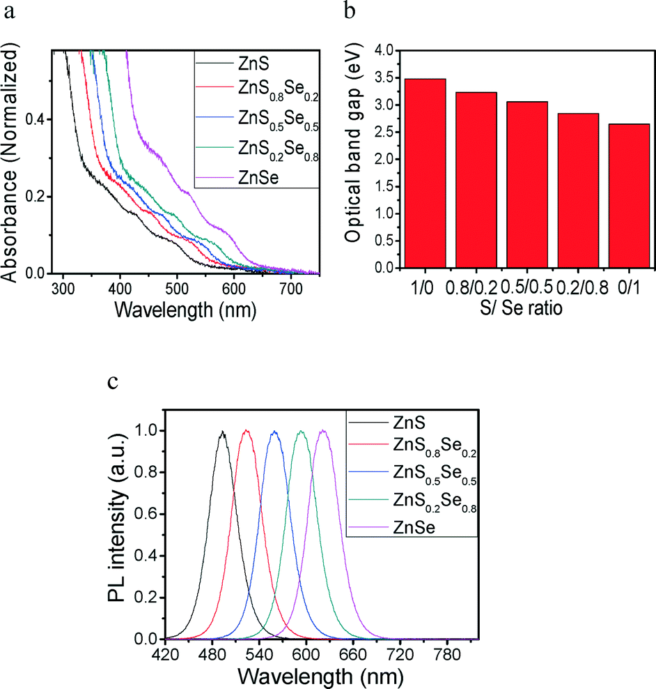 | ||
| Fig. 4 (a) UV–vis absorption spectra of ZnSxSe1−x nanofibers synthesized at various ratio values as functions of x = 1, 0.8, 0.5, 0.2 and 0. (b) Variation of band gap with ZnSxSe1−x nanofiber composition. (c) PL spectra of the ZnSxSe1−x nanofibers with various S/Se ratios dispersed in toluene. The S ratio decreases from left to right (1, 0.8, 0.5, 0.2 and 0). The excitation wavelength is 442 nm (x = 1 and 0.8) and 532 nm (x = 0.5, 0.2 and 0). | ||
Conclusions
A low-cost electrospinning synthetic approach for designing ZnSxSe1−x nanofibers offers a simple methodology for tuning the optical properties across the entire compositional range from pure ZnS to pure ZnSe. By varying the S:Se precursor ratio, we were able to tune the optical band gap of the ZnSxSe1−x nanofibers from 2.65 to 3.48 eV. These ZnSxSe1−x nanofibers were found to be highly crystalline wurtzite phase, and grew along the [0001] direction. A strong visible PL emission is estimated for ZnSxSe1−x showing an optical emission band from 490 to 630 nm. ZnSxSe1−x nanofibers have great potential applications in optoelectronics, photonic devices, photocatalysis, biosensors, drug targeting, diagnostic analysis and white light illumination sources.
Acknowledgements
The authors would like to thank the Ministry of Science and Technology, Taiwan (MOST) (contract 103-2112-M-006-016-MY3) and the Department of Photonics, National Cheng Kung University for supporting this research.Notes and references
- H. Li, X. Wang, J. Xu, Q. Zhang, Y. Bando, D. Golberg, Y. Ma and T. Zhai, Adv. Mater., 2013, 25, 3017 CrossRef CAS PubMed
.
- F. Shiba, T. Tamagawa, T. Kojima and Y. Okawa, CrystEngComm, 2013, 15, 1061 RSC
- R. Jing, A. Shan, R. Wang and C. Chen, CrystEngComm, 2013, 15, 3587 RSC
- X. T. Zhang, K. M. Ip, Z. Liu, Y. P. Leung, Q. Li and S. K. Hark, Appl. Phys. Lett., 2004, 84, 2641 CrossRef CAS PubMed
- S. Jana, B. B. Srivastava, S. Acharya, P. K. Santra, N. R. Jana, D. D. Sarmac and N. Pradhan, Chem. Commun., 2010, 46, 2853–2855 RSC
- P. Narang, S. Chen, N. C. Coronel, S. Gul, J. Yano, L. W. Wang, N. S. Lewis and H. A. Atwater, Adv. Mater., 2014, 26, 1235 CrossRef CAS PubMed
- A. Pan, R. Liu, M. Sun and C. Ning, J. Am. Chem. Soc., 2009, 131, 9502 CrossRef CAS PubMed
- L. J. Chen, J. D. Liao, Y. J. Chuang and Y. S. Fu, J. Am. Chem. Soc., 2011, 133, 3704 CrossRef CAS PubMed
- T. Trindade, P. O'Brien and N. L. Pickett, Chem. Mater., 2001, 13, 3843 CrossRef CAS
- V. Lesnyak, A. Dubavik, A. Plotnikov, N. Gaponik and A. Eychmüller, Chem. Commun., 2010, 46, 886–888 RSC
- A. Shavel, N. Gaponik and A. Eychmller, J. Phys. Chem. B, 2004, 108, 5905 CrossRef CAS
- Y. Zhang, H. Xu and Q. Wang, Chem. Commun., 2010, 46, 8941–8943 RSC
- X. Wu, P. Jiang, Y. Ding, W. Cai, S. S. Xie and Z. L. Wang, Adv. Mater., 2007, 19, 2319–2323 CrossRef CAS PubMed
- W. Jia, B. Jia, X. Wu and F. Qu, CrystEngComm, 2012, 14, 7759–7763 RSC
- W. Jia, B. Jia, F. Qu and X. Wu, Dalton Trans., 2013, 42, 14178–14187 RSC
- L. Hu, J. Yan, M. Liao, H. Xiang, X. Gong, L. Zhang and X. Fang, Adv. Mater., 2012, 24, 2305–2309 CrossRef CAS PubMed
- C. S. Tiwary, C. Srivastava and P. J. Kumbhakar, Appl. Phys., 2011, 110, 034908 Search PubMed
- L. H. Zhang, H. Q. Yang, J. Yu, F. H. Shao, L. Li, F. H. Zhang and H. J. Zhao, J. Phys. Chem. C, 2009, 113, 5434 CAS
- L. W. Yin and S. T. Lee, Nano Lett., 2009, 9, 957 CrossRef CAS PubMed
- M. Wang, G. T. Fei, Y. G. Zhang, M. G. Kong and L. D. Zhang, Adv. Mater., 2007, 19, 4491 CrossRef CAS PubMed
- Y. J. Chuang, J. D. Liao and L. J. Chen, J. Compos. Mater., 2012, 46, 227 CrossRef CAS PubMed
- L. J. Chen, J. D. Liao, Y. J. Chuang and Y. S. Fu, Polymer, 2011, 52, 116 CrossRef CAS PubMed
- J. M. Deitzel, J. Kleinmeyer, D. Harris and N. C. Beck Tan, Polymer, 2001, 42, 261 CrossRef CAS
- D. H. Reneker and I. Chun, Nanotechnology, 1996, 7, 216 CrossRef CAS
- S. G. Lee, S. S. Choi and C. W. Joo, J. Korean Fiber Soc., 2002, 39, 1 CAS
- P. Ruenraroengsak and A. T. Florence, Int. J. Pharm., 2005, 298, 361 CrossRef CAS PubMed
- M. R. Karim, H. W. Lee, R. Kim, B. C. Ji, J. W. Cho and T. W. Son, Carbohydr. Polym., 2009, 78, 336e42 CrossRef PubMed
- Y. Y. Chen and W. C. J. Wei, J. Eur. Ceram. Soc., 2001, 21, 2535e40 Search PubMed
- W. Liu, D. B. Mitzi, M. Yuan, A. J. Kellock, S. Jay Chey and O. Gunawan, Chem. Mater., 2010, 22, 3 CrossRef
- S. M. Kim, G. S. Kim and S. Y. Lee, Mater. Lett., 2008, 62, 4354 CrossRef CAS PubMed
- J. Baars and G. Brandt, J. Phys. Chem. Solids, 1973, 34, 905 CrossRef
- M. G. Panthani, V. Akhavan, B. Goodfellow, J. P. Schmidtke, L. Dunn, A. Dodabalapur, P. F. Barbara and B. A. Korgel, J. Am. Chem. Soc., 2008, 130, 16770 CrossRef CAS PubMed
- D. Pan, X. Wang, Z. H. Zhou, W. Chen, C. Xu and Y. Lu, Chem. Mater., 2009, 21, 2489 CrossRef CAS
- S. Shen, Y. Zhang, Y. Liu, L. Peng, X. Chen and Q. Wang, Chem. Mater., 2012, 24, 2407 CrossRef CAS
- S. Li, Z. Zhao, Q. Liu, L. Huang, G. Wang, D. Pan, H. Zhang and X. He, Inorg. Chem., 2011, 50, 11958 CrossRef CAS PubMed
- S. Mehta, S. Kumar, S. Chaudhary, K. Bhasin and M. Gradzielski, Nanoscale Res. Lett., 2009, 4, 17 CrossRef CAS PubMed
Footnote |
| † Electronic supplementary information (ESI) available: Synthesis and characterization details, thermogravimetric analysis (TGA) curves, X-ray diffraction (XRD) patterns and typical XPS spectra of the synthesized wurtzite ZnSxSe1−x nanofibers. See DOI: 10.1039/c5ce00477b |
| This journal is © The Royal Society of Chemistry 2015 |