
Domain matching epitaxy of GaN films on a novel langasite substrate: an in-plane epitaxial relationship analysis
Byung-Guon
Park
a,
R.
Saravana Kumar
a,
Moon-Deock
Kim
*a,
Hak-Dong
Cho
b,
Tae-Won
Kang
b,
G. N.
Panin
bc,
D. V.
Roschupkin
c,
D. V.
Irzhak
c and
V. N.
Pavlov
c
aDepartment of Physics, Chungnam National University, 220 Gung-dong, Yuseong-gu, Daejeon 305-764, South Korea. E-mail: mdkim@cnu.ac.kr; Fax: +82 42 822 8011; Tel: +82 42 821 5452
bDepartment of Physics, Quantum-functional Semiconductor Research Center, Dongguk University, Seoul 100-715, South Korea
cInstitute of Microelectronics Technology and High Purity Materials, Russian Academy of Sciences, Chernogolovka, Moscow 142432, Russia
First published on 20th May 2015
Abstract
We report the epitaxial growth of c-plane GaN films on a novel langasite (La3Ga5SiO14, LGS) substrate by plasma-assisted molecular beam epitaxy. The in-plane epitaxial relationship and the structural properties of GaN films on an LGS substrate were investigated using in situ reflective high energy electron diffraction (RHEED), high resolution X-ray diffraction (HR-XRD) and Raman spectroscopy. The in-plane epitaxial relationship between GaN and LGS determined using RHEED pattern was found to be GaN[10![[1 with combining macron]](https://www.rsc.org/images/entities/char_0031_0304.gif) 0]//LGS[21
0]//LGS[21![[3 with combining macron]](https://www.rsc.org/images/entities/char_0033_0304.gif) 0] and GaN[11
0] and GaN[11![[2 with combining macron]](https://www.rsc.org/images/entities/char_0032_0304.gif) 0]//LGS[14
0]//LGS[14![[5 with combining macron]](https://www.rsc.org/images/entities/char_0035_0304.gif) 0]. HR-XRD results confirmed the exact epitaxial relationship, and showed that six reflection peaks of GaN(102) were shifted around 19° from those of LGS(102). Raman analysis revealed that a minute compressive strain still existed in the GaN film due to the very small lattice mismatch between GaN and LGS. The results obtained in this study demonstrate that the nearly lattice-matched LGS can be a promising and futuristic substrate material for the growth of GaN, and it is foreseen that our results could be a reference for the further development of high performance nitride-based devices.
0]. HR-XRD results confirmed the exact epitaxial relationship, and showed that six reflection peaks of GaN(102) were shifted around 19° from those of LGS(102). Raman analysis revealed that a minute compressive strain still existed in the GaN film due to the very small lattice mismatch between GaN and LGS. The results obtained in this study demonstrate that the nearly lattice-matched LGS can be a promising and futuristic substrate material for the growth of GaN, and it is foreseen that our results could be a reference for the further development of high performance nitride-based devices.
1. Introduction
Materials of the III–V nitride semiconductor family have witnessed a massive evolution during the last two decades and are the basis of today's optoelectronic and microelectronic devices.1,2 In particular, GaN has attracted tremendous interest as a prospective material for high temperature, high power electronic and optoelectronic devices ranging from the visible to the ultraviolet (UV) region owing to its intrinsic properties like a large direct band gap (3.4 eV), excellent thermal conductivity, strong interatomic bond strength, good thermal stability, and the ability to tune its band gap from the UV to the infrared region by alloying with In and Al.3–6 Although GaN-based devices are successfully commercialized, the growth of high quality and crack-free GaN epilayers is still a challenging task. Since a sizable lattice-matched nitride substrate is not yet available for homoepitaxy, GaN is inevitably grown heteroepitaxially on foreign substrates like sapphire, SiC and more often on Si due to its low cost, good thermal and electrical conductivities, and the potential integration of GaN devices in well-established Si electronics.7,8 However, the large lattice mismatch and thermal expansion coefficient incompatibility between GaN and the substrates underneath induce a high density of threading dislocations (~109–1010 cm−2) and even cracking, which are big threats to the lifetime, reliability and yield of the GaN-based devices.9,10 Significant efforts aimed at alleviating the above issues have been proposed, among which the use of buffer layers or intermediate layers such as AlN,1 SixNy,10 low temperature GaN,11 an AlN/GaN superlattice structure,7,12 and graded AlxGa1−xN,12,13 has shown substantial improvement in the crystalline quality of GaN epilayers. In spite of this breakthrough in technologies involving the use of buffer layers, the grown GaN epilayers are quite inferior consisting of defects and cracks, and hence the growth of high quality and crack-free GaN epilayers still remains a formidable challenge. One innovative approach to circumvent this problem is to explore novel substrate materials that can compensate the lattice and thermal misfit between the overgrown GaN and the substrate beneath for realizing high performance GaN-based devices. Previously, T. Fukuda et al.14 regarded the langasite (LGS) family of materials as appropriate substrate materials for GaN heteroepitaxy due to their small lattice mismatch as well as domain matching epitaxy. LGS belongs to a trigonal crystal system with the space group P321, having a high melting point (1475 °C), an in-plane structure with hexagonal symmetry and the lattice constants a = 8.161 Å and c = 5.087 Å. Owing to its excellent piezoelectric properties it has been extensively used in surface acoustic wave (SAW) filters, and high temperature and high pressure sensor applications.15–17 Furthermore, the thermal expansion coefficient difference between GaN (5.59 × 10⁻⁶ K−1) and LGS (5.20 × 10⁻⁶ K−1) is very small (~7.5%) when compared to conventional substrates like sapphire (7.5 × 10⁻⁶ K−1, −25.5%) and 6H-SiC (4.2 × 10⁻⁶ K−1, 33.1%).17,18 Despite these potential virtues, LGS has been rarely used as a substrate for the growth of GaN epilayers.In light of this, in the present work GaN films were grown on a LGS substrate at a relatively low temperature (640 °C) using plasma-assisted molecular epitaxy (PA-MBE), and the in-plane epitaxial relationship between GaN and LGS was investigated in detail. This low temperature growth is highly desirable in the case of III-nitride growth since it suppresses the desorption of nitrogen atoms on the growing surface and increases the efficiency of In incorporation in InGaN/GaN LEDs and solar cells. Indeed, this is the first report demonstrating the successful growth of GaN films on a LGS substrate, and it can be anticipated that the present study will open up a new series of investigations addressing the challenges in GaN-based devices.
2. Experimental details
GaN thin films were grown on a LGS substrate (Fomos-Materials Co.) using PA-MBE equipped with an in situ reflection high energy electron diffraction (RHEED) set up. Gallium (Ga) was supplied by a standard Knudsen cell while active nitrogen (N2) was provided by a radio-frequency (RF) plasma source. Molybdenum was coated on the rear side of the LGS substrate to improve the consistency of heat transfer. Prior to the GaN growth, the substrate was cleaned sequentially in acetone, methanol and isopropyl alcohol for 5 min, and then rinsed in deionized water for 10 min. Then, the remnants of the water on the LGS substrate were thermally removed at 300 °C for 1 hr. An initial GaN nucleation layer of thickness 5 nm was grown at 480 °C on the LGS substrate, followed by the growth of a 620 nm GaN epilayer deposited at 640 °C with a growth rate of 0.33 monolayers/sec. The N2 flow rate, RF power, and Ga partial pressure were maintained at 3.0 sccm, 450 W, and 1.2 × 10⁻⁶ Torr, respectively. For comparison, a GaN thin film of the same thickness (660 nm) was deposited on a sapphire substrate by using an AlN buffer layer. The 35 nm thick AlN buffer layer was deposited at 792 °C on a nitridated sapphire substrate, and the N2 flow rate, RF power, and Al partial pressure were maintained at 1.5 sccm, 185 W, and 1.0 × 10⁻⁷ Torr, respectively. Then, the GaN thin films were deposited on the AlN/sapphire substrate under the same growth conditions used for growing the GaN epilayers on the LGS substrate.The crystallographic properties of the GaN films were investigated using high resolution X-ray diffraction (Bruker D8 X-ray Diffractometer, HR-XRD) and the growth process was monitored by in situ RHEED operating at 20 kV. The surface morphology of the GaN films was analyzed using a scanning electron microscope (SEM, Hitachi S 4800). Raman measurements were performed at room temperature in back-scattering geometry using the 532 nm line of an Ar+ laser (UniRAM-5500) to examine the strain state in the GaN films.
3. Results and discussion
It is essential to optimize the growth conditions as well as to examine their effects on the evolution of crystallization and surface morphology of GaN films on an LGS substrate in order to achieve crystal quality competing with that of conventional MOCVD-grown GaN. Hence, the evolution of GaN films on an LGS substrate was investigated by varying the growth conditions, namely the growth temperature (Tg) and the nucleation layer (Fig. 1). Fig. 1(a) and (b) shows the SEM images of GaN films grown on the LGS substrate at 570 °C and 610 °C, respectively, without any nucleation layer. Discontinuous coalesced islands of GaN crystals having a platelet-like morphology with a pronounced channel and hole structure were obtained, and their size increased with the increase in Tg. In situ RHEED observations (not shown) showed a diffused ring pattern indicating the formation of GaN islands. In contrast, the insertion of a low temperature GaN nucleation layer (Tg = 480 °C) significantly improved the surface features of subsequent GaN epilayers (Tg = 640 °C) grown on the LGS substrate. The SEM image in Fig. 1(c) shows the smooth and mirror-like surface of GaN epilayers on the LGS substrate. The RHEED patterns displayed well-defined streaky patterns demonstrating the two-dimensional (2D) growth mode of GaN (Fig. 2(a) and (b)). The cross-sectional SEM image (Fig. 1(d)) revealed good thickness uniformity and heterointerface quality, and the thickness of the GaN epilayers was measured to be around 620 nm. AFM observation (inset in Fig. 1(c)) showed steps and a terraced structure, and the root mean square (RMS) value for roughness of 1 × 1 μm2 scanning area was only 0.291 nm.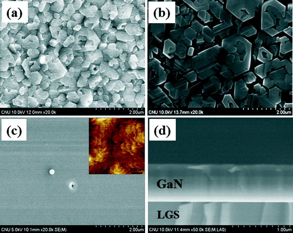 | ||
| Fig. 1 SEM images of GaN films grown on LGS at different Tg: (a) 570 °C and (b) 610 °C without a nucleation layer; (c) plane-view and (d) cross-sectional image of the GaN epilayers on the LGS substrate with a GaN nucleation layer (inset is the AFM image). | ||
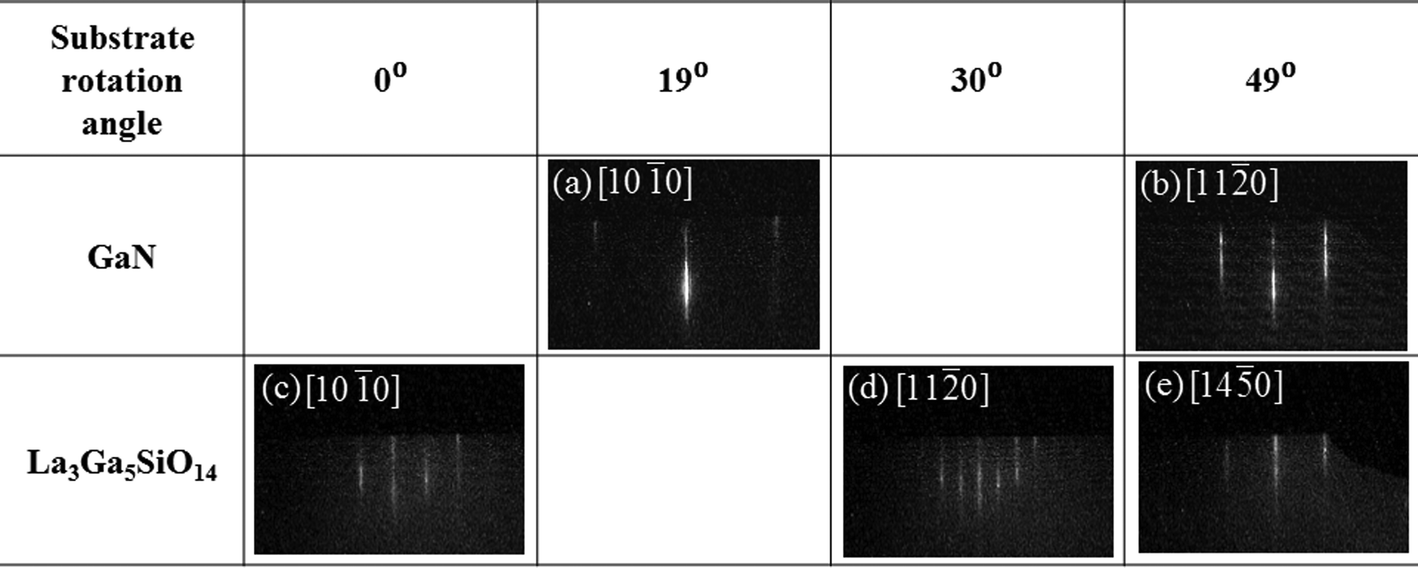 | ||
| Fig. 2 RHEED patterns of (a) and (b) the GaN film; and (c)–(e) the LGS substrate. | ||
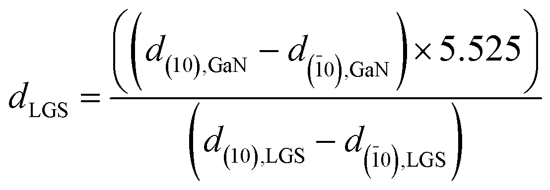
The in-plane epitaxial relationship between GaN and LGS was investigated by in situ RHEED, and is shown in Fig. 2. The streaky patterns in Fig. 2(a) and (b) obtained along the [100] and [110] azimuths after the growth of the GaN film indicates the 2D growth mode of GaN on LGS. Furthermore, the GaN film exhibited an identical RHEED pattern for every 60° rotation of the substrate. The [100] and [110] azimuths of the GaN film was found to be rotated by 19° with respect to the LGS [100] and [110] azimuths (Fig. 2(c) and (d)), respectively. The RHEED pattern of LGS in Fig. 2(e) displayed the same azimuth direction ([110]) as that of GaN[110]. Since no precise data for the LGS azimuth directions is available, the in-plane epitaxial relationship between GaN and LGS obtained using RHEED patterns is inadequate. However, to confirm the observed in-plane epitaxial relations, the azimuth directions of LGS were further determined using the lattice constants from the RHEED pattern. In general, a lattice parameter is the reciprocal of the in-plane lattice parameter, and hence the lattice spacing between the (10) and (0) diffraction streaks can be determined directly from the RHEED pattern. If the spacing between the (10) and (0) diffraction streaks of GaN[110] in Fig. 2(b) is 5.525 Å,19 then the lattice constant of LGS in Fig. 2(c)–(e) can be estimated using eqn (1),20
 | (1) |
0),GaN’ is the spacing between the streaks measured from the RHEED pattern of GaN[110] in Fig. 2(b), and ‘d(10),LGS − d(0),LGS’ is the spacing between the streaks measured from the RHEED patterns of LGS (Fig. 2(c)–(e)). The lattice constants of LGS estimated from Fig. 2(c), (d) and (e) were found to be 8.088 Å, 14.122 Å and 5.292 Å, respectively. When compared with the reported in-plane lattice constant of LGS (8.167 Å),21 the estimated lattice constant of LGS in Fig. 2(c) corresponds to the [100] azimuth direction of LGS. Since the in-plane structure of LGS is of hexagonal symmetry, the estimated lattice constant value of 14.122 Å for LGS in Fig. 2(d) corresponds to the [110] azimuth direction. The azimuth direction after a 19° rotation of the [110] azimuth can be estimated using eqn (2),22 | (2) |
0], the values of the second miller indices (h2k2(−k2−h2)0) are changed until the value equivalent to cos 19° was obtained. Based on the above calculations, the azimuth direction after rotation of the [110] azimuth of LGS by 19° was found to be [140], which is consistent with the RHEED pattern in Fig. 2(e). Similarly, the azimuth direction after a 19° rotation of the [100] azimuth of LGS was found to be [210]. Hence, these results suggest that the in-plane epitaxial relationships between GaN and LGS due to the lattice mismatch and crystallographic structure are GaN[100]//LGS[210] and GaN[110]//LGS[140].
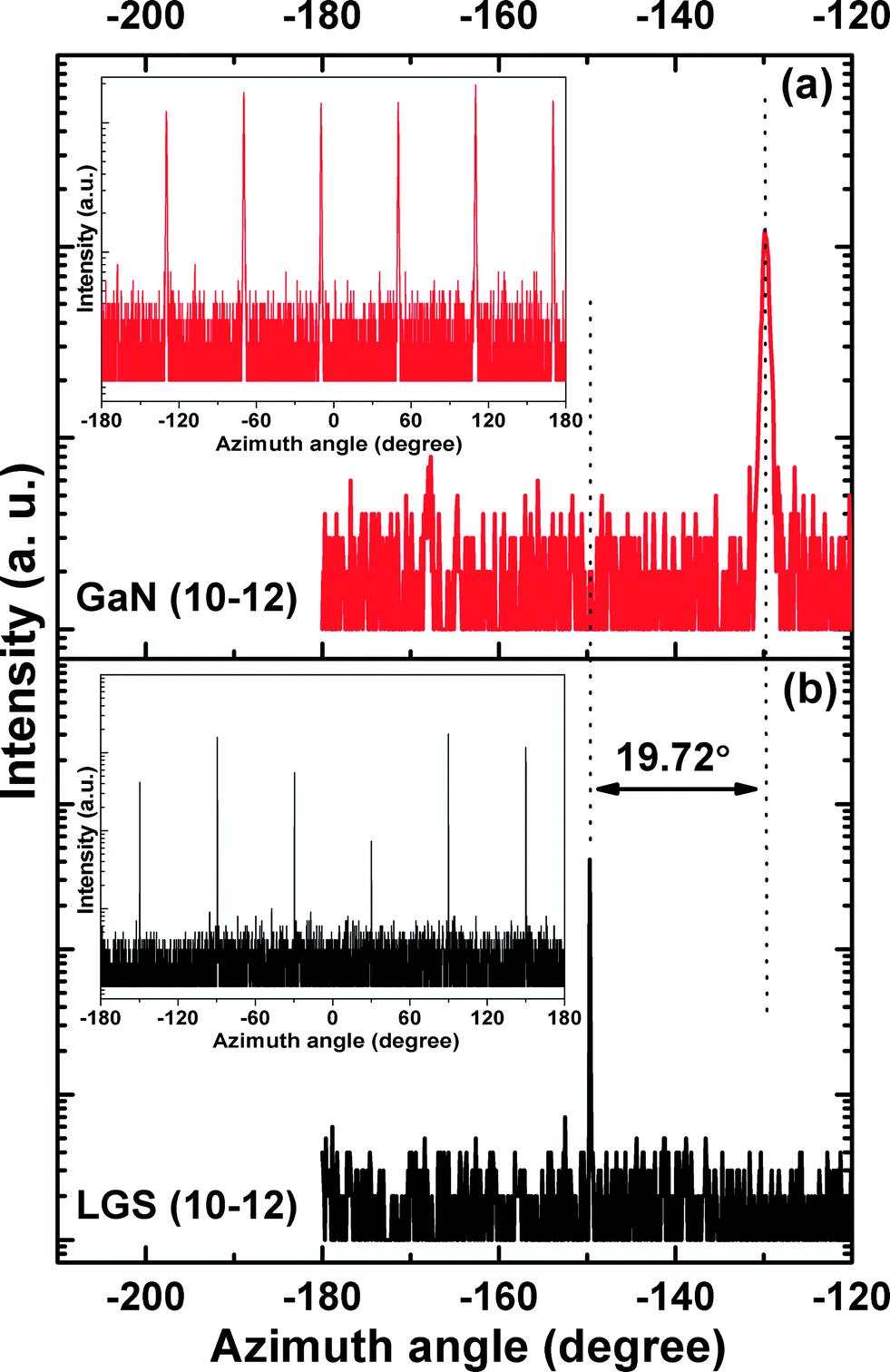
The Φ-scan XRD patterns of GaN(102) and LGS(102) were further used to confirm the exact epitaxial relationship, and are given in Fig. 3. The Φ-scan of the GaN(102) planes showed six reflection peaks rotated by 60° with respect to each other, clearly confirming the hexagonal structure of GaN (inset in Fig. 3(a)). Also, the Φ-scan of the GaN(102) planes showed similar reflection peaks to those of the LGS(102) planes. The first reflection peaks of the LGS(102) and GaN(102) planes were observed at the 149.67° and 129.95° azimuth angles, respectively, which indicates that six reflection peaks of GaN(102) planes were shifted by 19.72° with respect to LGS(102). These observations are in fairly good agreement with the in-plane epitaxial relationship deduced from the RHEED patterns.
 | ||
| Fig. 3 Full range Φ-scan patterns of (a) the GaN(102) and (b) the LGS(102) reflection planes (insets show the first reflection peaks of GaN(102) and LGS(102)). | ||
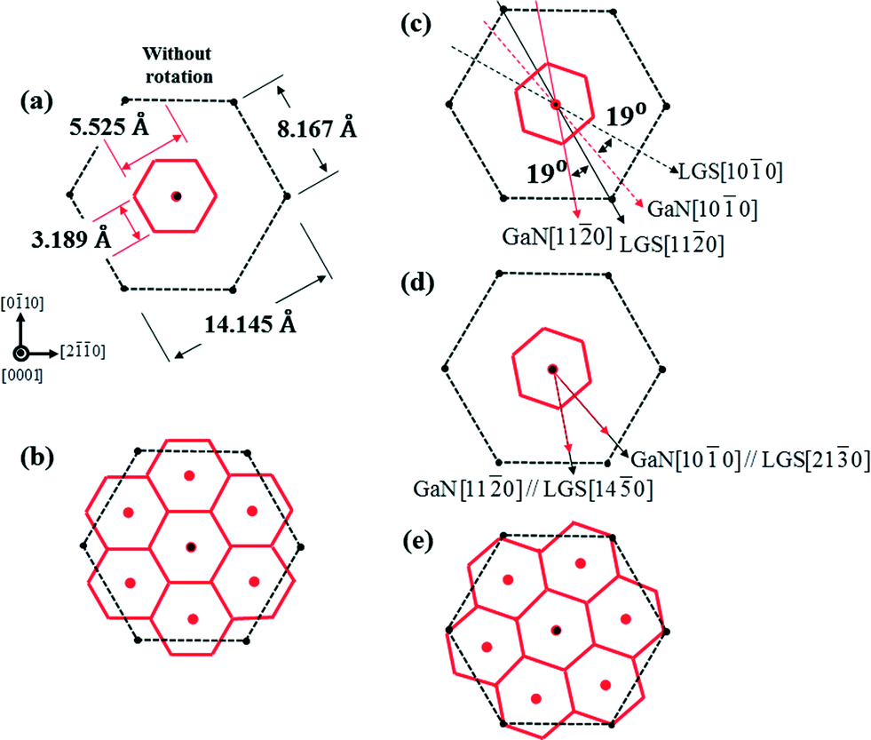
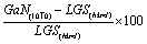
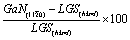
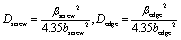
Based on the observations from RHEED and the Φ-scan XRD patterns, the in-plane alignment of GaN on LGS is schematically shown in Fig. 4. Fig. 4(a) shows the in-plane hexagonal unit cells of LGS and GaN. Fig. 4(b) illustrates that seven unit cells of GaN approximately corresponds to one unit cell of LGS. When GaN is not rotated with respect to LGS, the lattice mismatch between GaN[100] and LGS[100] is −60.9%. If the lattice constant of GaN is increased twofold and threefold to match the lattice constant of LGS, the lattice mismatch between LGS and GaN is reduced to −21.9% and +17.1%, respectively, which is still high.14Fig. 4(c) shows the 19° rotation of the GaN [100] and [110] azimuths with respect to the LGS [100] and [110] azimuths, respectively. When GaN is rotated by 19° with respect to LGS, the azimuth directions of GaN [100] and [110] become parallel to the LGS [210] and [140] azimuths, respectively (Fig. 4(d)). The in-plane alignment of the seven unit cells of GaN (Fig. 4(e)) after a 19° rotation closely matches with one unit cell of LGS.
 | ||
| Fig. 4 Schematic diagrams showing: (a) the in-plane lattices of GaN and LGS; and (b)–(e) the in-plane alignment of GaN on LGS. | ||
The lattice mismatches calculated using the interplanar distances from the standard JCPDS data of GaN (card no. 50-0792) and LGS (card no. 41-0155) are given in Table 1. It can be seen from the table that the lattice mismatch was minimum along GaN(100) and LGS(210), as well as along the GaN(110) and LGS(140) directions. The estimated lattice mismatch value of 3.2% indicates a compressive strain in GaN. Moreover, the planes of LGS(210) and LGS(140) were positioned at 19.1° from LGS(100) and LGS(110), respectively. The calculated values of the lattice mismatch and rotation angle are consistent with the experimental results of RHEED and the Φ-scan. Therefore, it seems reasonable to conclude that GaN is rotated by 19° from LGS[100] or LGS[110] due to the lattice mismatch. Similarly, in the case of GaN on sapphire with an in-plane epitaxial relationship of GaN(100)//sapphire(110), the unit cell of GaN was rotated by 30° with respect to sapphire due to the large lattice mismatch (~14%).23
| Miller index (hkml) | Rotation angle (degrees) | Lattice spacing (Å) | Lattice mismatch (%) | ||
|---|---|---|---|---|---|
| LGS | GaN |
|
|
||
| (100) |
0 | 7.7080 | 2.7618 | −60.981 | −77.472 |
| (210) |
19.10 | 2.6752 | 1.0438 | 3.237 | −40.397 |
| (110) |
30.00 | 4.0865 | 1.5945 | −32.416 | −60.981 |
| (140) |
49.10 | 1.5445 | 0.6026 | 78.815 | 3.237 |
The crystallographic properties of the GaN films were further analyzed using 2θ-ω scans and ω rocking curves using HR-XRD measurements. Besides the (0001) reflections from the LGS substrate, the 2θ-ω XRD spectrum of the GaN film (Fig. 5(a)) shows diffraction peaks corresponding to the (0002) and (0004) planes at 34.555° and 72.830°, respectively, indicating the single phase wurtzite crystal structure of GaN. Compared with the bulk GaN (2θ ~ 34.570°), the (0002) reflection from GaN (Fig. 5(b)) on the LGS substrate exhibits a slight shift towards a lower angle suggesting a compressive stress.8 The full width at half maximum (FWHM) of the rocking curves generally associated with the threading dislocation (TD) density is shown in Fig. 5(c) for the (0002) rocking curve, and was found to be 828 arcsec (0.23°). Although this value is little mediocre, it is reasonable when compared to the previously achieved ones on novel substrates or templates.24–29 The X-ray linewidth arises from the local tilting of reflection planes with respect to the substrate due to the crystal imperfections like dislocations and point defects in heteroepitaxially grown films, and is strongly dependent on the amount of the structural defects. In order to quantify the crystal imperfections further, the TD densities were estimated from the FWHM of the rocking curves of different on-axis symmetric (00l) and off-axis asymmetric (h0l) planes. It is well known that the FWHM of rocking curves of symmetric (00l) planes is related to the screw and mixed-type TDs, whereas that of asymmetric (h0l) planes represents the pure edge TDs, and in epitaxial GaN films the edge dislocation density (~1010 cm−2) is usually higher than the screw dislocation density (~108 cm−2).26,30 Using the FWHM of the X-ray rocking curves of the symmetric (002), (004), (006) and asymmetric (101), (102), (103), (302) planes, the screw and edge dislocation densities of the GaN films grown on the LGS and sapphire substrates were calculated using the following equation:26,31
 | (3) |
 | ||
| Fig. 5 2θ-ω Scans: (a) full range, and (b) GaN (0002) peak; (c) X-ray rocking curve of the GaN film on the LGS substrate. | ||
Where, ‘Dscrew’ is the screw dislocation density, ‘Dedge’ is the edge dislocation density, ‘βscrew’ is the slope for the symmetric reflection obtained from the Williamson–Hall plot, ‘βscrew’ is the FWHM at 90° of inclination from the skew scan for the asymmetric reflection, and ‘b’ is the Burgers vector length (bscrew = 0.5185 nm and bedge = 0.3189 nm). The edge and screw dislocation densities of the GaN film grown on the LGS substrate were found to be 3.7 × 10¹⁰ and 1.6 ×109 cm−2, respectively. For GaN on the sapphire substrate, the edge and screw dislocation densities were found to be 6.5 × 10⁹ and 5.9 × 108 cm−2, respectively. The dislocation densities of GaN on the LGS substrate were found to be one or two orders of magnitude higher when compared to the sapphire substrate or the earlier reports.26,32,33 Although the FWHM and dislocation density values of GaN grown on the LGS substrate are mediocre when compared to the GaN films grown on conventional substrates, it is expected that further optimization of growth conditions like growth temperature, thickness, buffer layer, and V-III ratio will undoubtedly address the difficulties of growing better quality GaN films on LGS, the study into which is currently underway.
Fig. 6 shows the Raman spectrum of the GaN films grown on the LGS and sapphire substrates. Both the samples exhibited similar Raman spectra, mainly composed of E2(high) and A1(LO) phonon modes of wurtzite GaN. The E2(high) and A1(LO) phonon modes of GaN grown on LGS were observed at 567.4 and 733.4 cm−1, respectively. Similarly, for GaN on sapphire, the E2(high) and A1(LO) phonon modes were observed at 570.9 and 734.5 cm−1, respectively. The E2(high) mode is generally used to estimate the stress in GaN epilayers as it is very sensitive to biaxial stress. A blue-shift in the E2(high) phonon peak indicates a compressive stress, while a red-shift indicates a tensile stress. In the present cases, the GaN film grown on both LGS as well as sapphire (inset in Fig. 6) exhibited a blue-shift in the E2(high) peak position when compared to stress-free GaN (567.2 cm−1), indicating a compressive stress.34 Nevertheless, the GaN film grown on the LGS substrate exhibited a minuscule frequency shift compared to the one grown on the sapphire substrate due to the small lattice mismatch between GaN[100] and LGS[210]. The in-plane compressive stress in GaN films was quantitatively evaluated using the relation Δω = kσ, where ‘Δω’ is the shift in the frequency of the phonon, ‘k’ is the Raman stress coefficient (4.3 cm−1 GPa−1), and ‘σ’ is the stress.35 The calculated stress in the GaN film on the LGS and sapphire substrates was 0.047 and 0.881 GPa, respectively.
 | ||
| Fig. 6 Raman spectra of the GaN films grown on the LGS and sapphire substrates. The inset is the magnified region of the E2(high) phonon peak. The vertical line indicate the peak position of unstrained GaN. | ||
4. Conclusions
In summary, we demonstrated the successful growth of GaN films on a nearly lattice-matched LGS substrate by PA-MBE. The morphology, crystalline quality, orientation and strain states in GaN films were assessed using SEM, HR-XRD, RHEED and Raman analyses. Experimental results revealed that GaN grown on LGS is almost stress-free with its lattice planes rotated by 19° with respect to LGS, having the in-plane epitaxial relationship of GaN[100]//LGS[210] and GaN[110]//LGS[140]. These are early results on the epitaxial growth of GaN films on an LGS substrate showing the feasibility of using LGS as a novel substrate material for GaN heteroepitaxy. In addition, we can expect that our results will open up the possibilities of using LGS substrate for the growth of other III-nitrides in the near future.
Acknowledgements
This research was supported by the leading foreign research institute recruitment program through the National Research Foundation for Korea (NRF) funded by the Ministry of Education, Science and Technology (MEST, no. 2014-039452). Also this research was supported through the International Research and Development Program of the NRF of Korea funded by the MEST (no. 2014-073957).References
- Y. H. Wu, C. H. Lee, C. M. Chu, Y. H. Yeh, C. L. Chen and W. I. Lee, 08JB08, Jpn. J. Appl. Phys., 2013, 52 Search PubMed
.
- P. Gupta, A. A. Rahman, N. Hatui, M. R. Gokhale, M. M. Deshmukh and A. Bhattacharya, J. Cryst. Growth, 2013, 372, 105 CrossRef CAS PubMed
- D. C. Oh, S. W. Lee, H. Goto, S. H. Park, I. H. Im, T. Hanada, M. W. Cho and T. Yao, Appl. Phys. Lett., 2007, 91, 132112 CrossRef PubMed
- A. Khan, K. Balakrishnan and T. Katona, Nat. Photonics, 2008, 2, 77 CrossRef CAS PubMed
- Y. Fujita, Y. Takano, Y. Inoue, M. Sumiya, S. Fuke and T. Nakano, 08JB26, Jpn. J. Appl. Phys., 2013, 52 Search PubMed
- H. Li, L. Zhang, Y. Shao, Y. Wu, X. Hao, H. Zhang, Y. Dai and Y. Tian, Int. J. Electrochem. Sci., 2013, 8, 4110 CAS
- X. Q. Shen, T. Takahashi, X. Rong, G. Chen, X. Q. Wang, B. Shen, H. Matsuhata, T. Ide and M. Shimizu, Appl. Phys. Lett., 2013, 103, 231908 CrossRef PubMed
- J. Wang, H. B. Ryu, M. S. Park, W. J. Lee, Y. J. Choi and H. Y. Lee, J. Cryst. Growth, 2013, 370, 249 CrossRef CAS PubMed
- J. Ma, X. Zhu, K. M. Wong, X. Zou and K. M. Lau, J. Cryst. Growth, 2013, 370, 265 CrossRef CAS PubMed
- T. Y. Wang, S. L. Ou, R. H. Horng and D. S. Wuu, J. Cryst. Growth, 2014, 399, 27 CrossRef CAS PubMed
- H. Xu, X. Hu, X. Xu, Y. Shen, S. Qu, C. Wang and S. Li, Appl. Surf. Sci., 2012, 258, 6451 CrossRef CAS PubMed
- L. Ravikiran, M. Agrawal, N. Dharmarasu and K. Radhakrishnan, 08JE05, Jpn. J. Appl. Phys., 2013, 52 Search PubMed
- M. H. Kim, Y. G. Do, H. C. Kang, D. Y. Noh and S. J. Park, Appl. Phys. Lett., 2001, 79, 2713 CrossRef CAS PubMed
- T. Fukuda, K. Shimamura, V. V. Kochurikhin, V. I. Chani, B. M. Epelbaum, S. L. Baldochi, H. Takeda and A. Yoshikawa, J. Mater. Sci.: Mater. Electron., 1999, 10, 571 CrossRef CAS
- O. A. Gurbanova and E. L. Belokoneva, Crystallogr. Rep., 2006, 51, 577 CrossRef CAS
- C. Klemenz, J. Cryst. Growth, 2002, 237–239, 714 CrossRef CAS
- J. Kraublich, S. Hofer, U. Zastrau, N. Jeutter and C. Baehtz, Cryst. Res. Technol., 2010, 45, 490 CrossRef PubMed
- H. Lahreche, M. Leroux, M. Laugt, M. Vaille, B. Beaumont and P. Gibart, J. Appl. Phys., 2000, 87, 577 CrossRef CAS PubMed
- H. Y. Chen, H. W. Lin, C. H. Shen and S. Gwo, Appl. Phys. Lett., 2006, 89, 243105 CrossRef PubMed
- Y. Liu, M. H. Xie, Y. G. Cao, H. S. Wu and S. Y. Tong, J. Appl. Phys., 2005, 97, 023502 CrossRef PubMed
- H. Ohsato, T. Iwataki and H. Morikoshi, Trans. Electr. Electron. Mater., 2012, 13, 51 CrossRef
-
B. D. Cullity and S. R. Stock, Elements of X-ray Diffraction, Prentice-hall, New Jersey, 3rd edn., 2001, p. 634 Search PubMed
- S. S. Kushvaha, M. Senthil Kumar, K. K. Maurya, M. K. Dalai and N. D. Sharma, AIP Adv., 2013, 3, 092109 CrossRef PubMed
- C. Liu, X. Gao, D. Tao, J. Wang and Y. Zeng, J. Alloys Compd., 2015, 618, 533 CrossRef CAS PubMed
- B. R. Yeom, R. Navamathavan, J. H. Park, Y. H. Ra and C. R. Lee, CrystEngComm, 2012, 14, 5558 RSC
- J. K. Jeong, H. J. Kim, H. C. Seo, H. J. Kim, E. Yoon, C. S. Hwang and H. J. Kim, Electrochem. Solid-State Lett., 2004, 7, C43 CrossRef CAS PubMed
- Y. J. Sun, O. Brandt, U. Jahn, T. Y. Liu, A. Trampert, S. Cronenberg, S. Dhar and K. H. Ploog, J. Appl. Phys., 2002, 92, 5714 CrossRef CAS PubMed
- J. Leathersich, E. Arkun, A. Clark, P. Suvarna, J. Marini, R. Dargis and F. (Shadi) Shahedipour-Sandvik, J. Cryst. Growth, 2014, 399, 49 CrossRef CAS PubMed
- E. Richter, Ch. Hennig, U. Zeimer, M. Weyers, G. Tränkle, P. Reiche, S. Ganschow, R. Uecker and K. Peters, Phys. Status Solidi C, 2006, 3, 1439 CrossRef CAS PubMed
- E. Arslan, O. Duygulu, A. A. Kaya, A. Teke, S. Ozcelik and E. Ozbay, Superlattices Microstruct., 2009, 46, 846 CrossRef CAS PubMed
- M. W. Cho, A. Setiawan, H. J. Ko, S. K. Hong and T. Yao, Semicond. Sci. Technol., 2005, 20, S13 CrossRef CAS
- H. Long, Y. Wei, T. Yu, Z. Wang, C. Jia, Z. Yang, G. Zhang and S. Fan, CrystEngComm, 2012, 14, 4728–4731 RSC
- P. Drechsel and H. Riechert, J. Cryst. Growth, 2011, 315, 211 CrossRef CAS PubMed
- Z. Lin, J. Zhang, R. Cao, W. Ha, S. Zhang, X. Chen, J. Yan, S. Xu, Y. Zhao, L. Li and Y. Hao, J. Cryst. Growth, 2013, 384, 96 CrossRef CAS PubMed
- M. Kawwam and K. Lebbou, Appl. Surf. Sci., 2014, 292, 906–914 CrossRef CAS PubMed
| This journal is © The Royal Society of Chemistry 2015 |